Scientists Sculpt Einstein Onto a Crystal Using only Light
Why It Matters
The ability to inscribe high‑contrast, sub‑micron optical features with simple lasers cuts manufacturing cost and complexity, accelerating the rollout of next‑generation photonic devices and secure anti‑counterfeiting tags.
Key Takeaways
- •As₂S₃ shows Δn≈0.3 under low‑intensity UV light
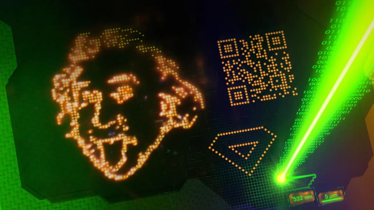
- •CW laser writes 700 nm spaced Einstein portrait in crystal
- •Material expands up to 5% when illuminated, enabling microlenses
- •Patterning resolution reaches ~50,000 dpi (≈500 nm spacing)
- •No cleanroom or femtosecond lasers required for nanoscale structuring
Pulse Analysis
The discovery of a giant photorefractive response in arsenic trisulfide reshapes expectations for van der Waals semiconductors. Traditional photorefractive crystals such as BaTiO₃ or LiNbO₃ deliver index changes an order of magnitude lower, limiting their utility for high‑resolution waveguide writing. By leveraging a simple continuous‑wave ultraviolet source, the XPANCEO team achieved a Δn of roughly 0.3, a value that rivals or exceeds many engineered nonlinear materials. This breakthrough underscores the growing relevance of layered chalcogenides, whose weak interlayer forces permit rapid, reversible structural modifications when illuminated.
Beyond the raw physics, the practical implications are far‑reaching. Direct‑write patterning at 700 nm spacing—demonstrated with an Einstein portrait—opens a low‑cost pathway to embed optical fingerprints in transparent substrates. Such high‑contrast, sub‑micron features can serve as tamper‑evident security marks, ultra‑dense data storage, or bespoke diffractive elements for augmented‑reality displays. The observed 5 % photomechanical expansion further enables on‑demand fabrication of microlenses and diffraction gratings, critical components for smart contact lenses and compact waveguide arrays. By eliminating the need for cleanroom lithography, manufacturers can accelerate prototyping cycles and reduce capital expenditures.
Industry analysts see this as a catalyst for a new generation of light‑only photonic architectures. As supply chains for femtosecond laser systems remain constrained, a CW‑laser‑based approach democratizes access to advanced optical manufacturing, especially for startups targeting anti‑counterfeiting, biomedical sensing, and consumer optics. Continued research into the durability and scalability of As₂S₃ patterning will determine its market penetration, but the current results suggest a rapid shift toward more sustainable, electrically independent photonic devices.
Scientists sculpt Einstein onto a crystal using only light
Comments
Want to join the conversation?
Loading comments...