Self‐Strain Suppression of the Metal‐to‐Insulator Transition in Phase‐Change Oxide Devices
•January 22, 2026
0
Why It Matters
Strain‑driven suppression of the MIT provides a scalable method to tune transition thresholds, directly impacting the design of low‑power, memory‑embedded neuromorphic devices.
Key Takeaways
- •Ion irradiation lowers V2O3 transition temperature
- •Strain mismatch suppresses metal‑insulator transition
- •Suppression occurs within irradiated region or edges
- •Effect intensifies as device dimensions shrink
- •Findings guide nanoscale phase‑engineering for neuromorphic chips
Pulse Analysis
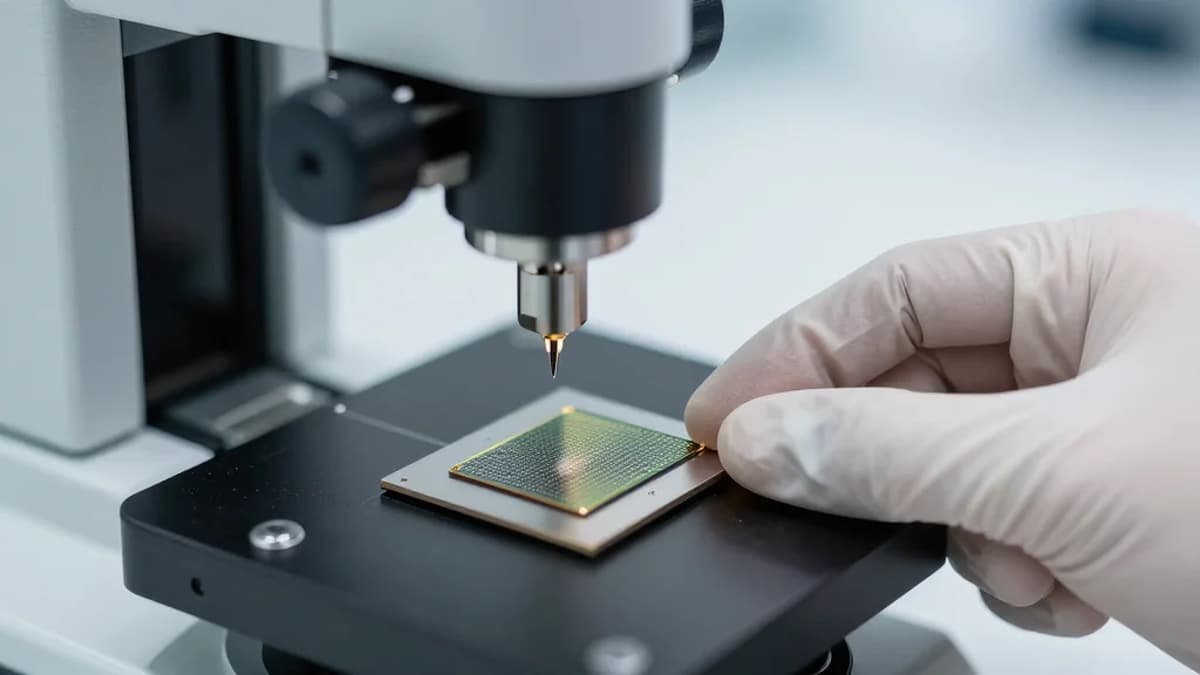
Phase‑change oxides such as vanadium sesquioxide (V2O₃) have attracted intense interest because their strongly correlated electrons enable abrupt metal‑to‑insulator transitions (MIT) that can be toggled by temperature, electric field, or optical pulses. Unlike conventional silicon transistors, these materials embed a structural memory element, making them attractive for neuromorphic architectures that mimic synaptic plasticity. The corundum‑to‑monoclinic transformation in V₂O₃ occurs near 150 °C, and controlling its critical temperature is essential for reliable spiking behavior in artificial neurons. These attributes also open pathways for low‑power, non‑volatile logic.
Using X‑ray nano‑diffraction, researchers imaged V₂O₃ micro‑devices with nanometer resolution, revealing how a focused gallium ion beam creates a localized defect region that lowers the MIT temperature. The lattice mismatch between pristine and irradiated zones generates internal strain, which in turn suppresses the phase transition either throughout the damaged area or along its perimeter, depending on defect distribution and feature size. This self‑straining mechanism demonstrates that mechanical stresses, often overlooked, can dominate the electronic response when device dimensions approach the nanoscale. The strain field can be mapped in real time, guiding device layout.
The discovery has immediate ramifications for scaling phase‑change memory and neuromorphic chips. As transistors shrink, built‑in strain becomes a design lever rather than a parasitic effect, enabling engineers to fine‑tune transition thresholds without additional circuitry. Moreover, the principle extends to other correlated oxides, suggesting a universal pathway for phase‑engineering through controlled irradiation or epitaxial strain. Future work will likely explore combinatorial stress‑electric field tuning, reliability under repeated cycling, and integration with CMOS back‑end processes, positioning strain‑mediated MIT control as a cornerstone of next‑generation computing. Industry roadmaps already cite strain‑engineered MIT as a key enabler for AI accelerators.
Self‐Strain Suppression of the Metal‐to‐Insulator Transition in Phase‐Change Oxide Devices
0
Comments
Want to join the conversation?
Loading comments...