Shrinking 2D Nanoribbons to 35 Nm Boosts Transistor Current
Why It Matters
The breakthrough demonstrates that aggressive width scaling of 2D semiconductor channels can enhance, not degrade, key transistor metrics, opening a viable path for ultra‑dense, high‑performance logic beyond silicon. This could extend Moore’s law by enabling next‑generation 3‑D architectures such as gate‑all‑around nanoribbons and CFETs.
Key Takeaways
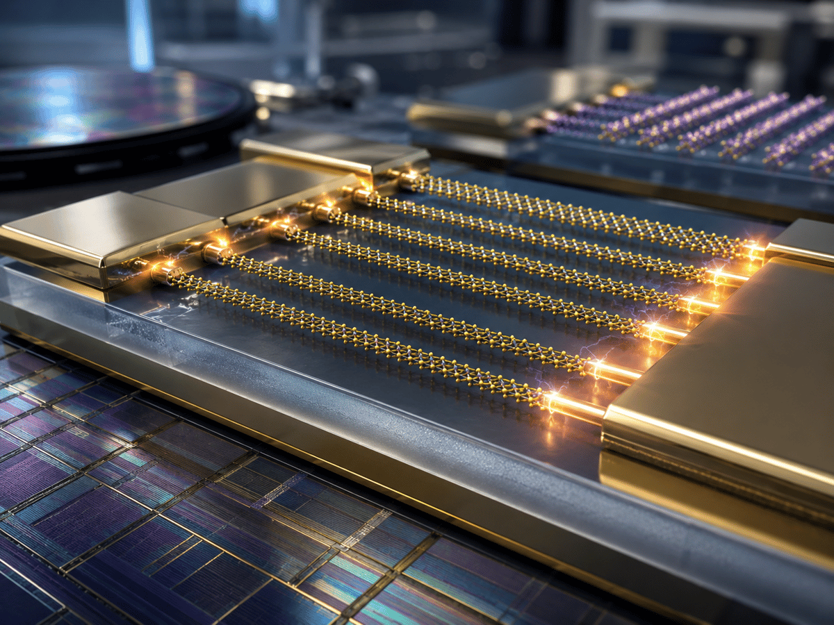
- •35 nm MoS₂ nanoribbons boost on‑current density by ~42 %
- •Subthreshold swing improves 16 % as width shrinks to 35 nm
- •Contact resistance drops from ~860 Ω·µm to ~270 Ω·µm
- •Edge passivation during etching preserves crystal quality
- •Scaling works for WS₂ n‑type and WSe₂ p‑type devices
Pulse Analysis
The semiconductor industry has long relied on silicon scaling to drive performance gains, but as gate lengths approach the sub‑10 nm regime, planar devices encounter fundamental limits such as short‑channel effects and variability. Two‑dimensional (2D) materials, especially transition‑metal dichalcogenides, offer atomically thin channels with inherent surface passivation, making them attractive candidates for next‑generation three‑dimensional architectures like gate‑all‑around nanoribbons and complementary FET stacks. However, the impact of aggressively narrowing these channels remained uncertain, with concerns that edge disorder would outweigh any electrostatic benefits.
The new Nature Communications study provides a systematic experimental validation that shrinking TMD nanoribbons to roughly 35 nm not only preserves device integrity but actively improves performance. MoS₂ ribbons achieve a peak on‑current density near 995 µA µm⁻¹, a 42 % boost over wider counterparts, while subthreshold swing tightens by 16 %. The authors attribute these gains to three intertwined mechanisms: intensified electric fields at the ribbon edges that enhance carrier accumulation, a three‑fold reduction in contact resistance due to more efficient side‑contact injection, and inadvertent oxygen passivation during Cl₂/O₂ plasma etching that mitigates sulfur‑vacancy traps. Even though carrier mobility dips modestly, the net effect is a superior transistor profile that challenges the conventional trade‑off between scaling and performance.
Beyond the laboratory, these findings have immediate relevance for industry roadmaps targeting sub‑5 nm logic nodes. By confirming that channel width is a powerful lever for electrostatic control without incurring prohibitive disorder, the work paves the way for integrating 2D nanoribbons into heterogeneous stacks alongside silicon, potentially extending Moore’s law through vertical scaling. Future research will need to push widths below 20 nm, refine edge‑smoothness, and align manufacturing processes with existing fab lines, but the demonstrated performance envelope suggests that 2D nanoribbon transistors could become a cornerstone of ultra‑dense, low‑power electronics in the coming decade.
Shrinking 2D Nanoribbons to 35 nm Boosts Transistor Current
Comments
Want to join the conversation?
Loading comments...