Sliding‐Ferroelectric hBN Bilayer Controlled Carrier Lifetimes in TMD Heterostructures
Why It Matters
The ability to reversibly program carrier lifetimes with atomic‑scale ferroelectric switching opens a pathway to reconfigurable optoelectronic and information‑processing devices, enhancing performance flexibility without altering material composition.
Key Takeaways
- •Switching hBN stacking changes interfacial potential direction
- •Carrier lifetimes vary from 1.5 ns to 74 ns across configurations
- •Low‑frequency shear/breathing phonons extend recombination times
- •High‑frequency intralayer optical phonons accelerate carrier decay
Pulse Analysis
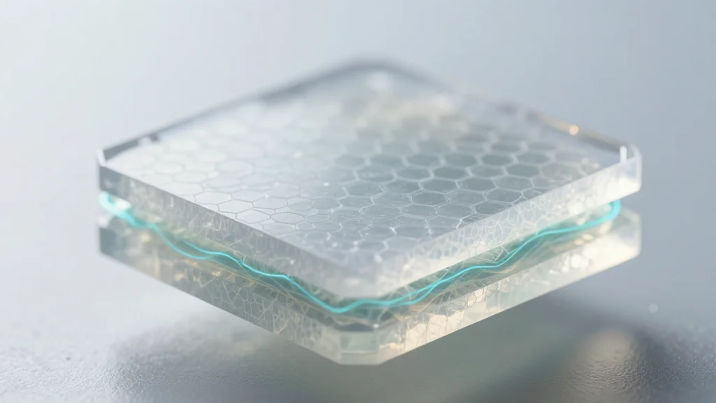
Sliding ferroelectricity in bilayer hBN introduces a uniquely sharp, non‑volatile electric field at the interface of two‑dimensional (2D) stacks. Unlike conventional ferroelectrics that rely on bulk domain switching, the relative translation of two atomically thin hBN sheets toggles a built‑in dipole, offering a reversible, nanoscale knob for engineering van der Waals heterostructures. This capability is especially valuable for transition‑metal‑dichalcogenide (TMD) platforms, where interfacial charge transfer dictates photodetection, light emission, and valleytronic functionalities.
In the study, time‑dependent density functional theory (TD‑DFT) paired with nonadiabatic molecular dynamics (NAMD) quantified how the AA′ (non‑polar) and AB/BA (ferroelectric) stackings reshape the electronic landscape of MoSe₂/hBN and WSe₂/hBN assemblies. The ferroelectric configuration flips the interfacial potential step, reversing charge‑transfer direction and modulating nonadiabatic coupling strengths. Consequently, carrier recombination times stretch from a few nanoseconds in the polar state to tens of nanoseconds in the non‑polar state, a more than 50‑fold tunability that rivals traditional doping or strain engineering.
These findings provide concrete design rules for next‑generation 2D optoelectronic circuits. By selecting specific phonon modes—low‑frequency interlayer shear and breathing vibrations for longer lifetimes, or high‑frequency intralayer optical phonons for rapid decay—engineers can tailor device speed, quantum efficiency, and energy consumption on demand. The reconfigurable nature of sliding‑ferroelectric hBN also suggests adaptive hardware for neuromorphic computing and programmable photonic logic, where dynamic control of carrier dynamics is a prerequisite. Future work will need to address scalability, integration with existing silicon platforms, and long‑term stability under operational cycling, but the demonstrated order‑of‑magnitude lifetime control marks a significant stride toward practical ferroelectric‑semiconductor hybrids.
Sliding‐Ferroelectric hBN Bilayer Controlled Carrier Lifetimes in TMD Heterostructures
Comments
Want to join the conversation?
Loading comments...