Strain Creates Moiré 2D Materials without Twisting or Stacking, Opening More Scalable Route
Why It Matters
The approach makes moiré‑engineered quantum materials compatible with existing semiconductor fabs, dramatically lowering the barrier to commercial devices that exploit exotic electronic phases.
Key Takeaways
- •Strain engineering replaces twisting for creating moiré superlattices
- •Lithographically patterned stressor films induce biaxial and uniaxial strain in MoS₂
- •Resulting polar domains enable electric-field tunable nanoscale resistance
- •Technique leverages standard semiconductor manufacturing steps, boosting scalability
- •Researchers aim to integrate strain‑induced moiré patterns into electronic devices
Pulse Analysis
The discovery of superconductivity in twisted bilayer graphene in 2018 sparked a wave of research into moiré‑engineered quantum materials. By deliberately misaligning atomically thin layers, scientists can reshape electronic band structures, unlocking correlated insulating states, magnetism and exotic superconductivity. However, the conventional method of manually rotating and stacking flakes suffers from low yield, high variability, and limited compatibility with wafer‑scale production. As a result, translating laboratory breakthroughs into commercial technologies has remained a formidable challenge.
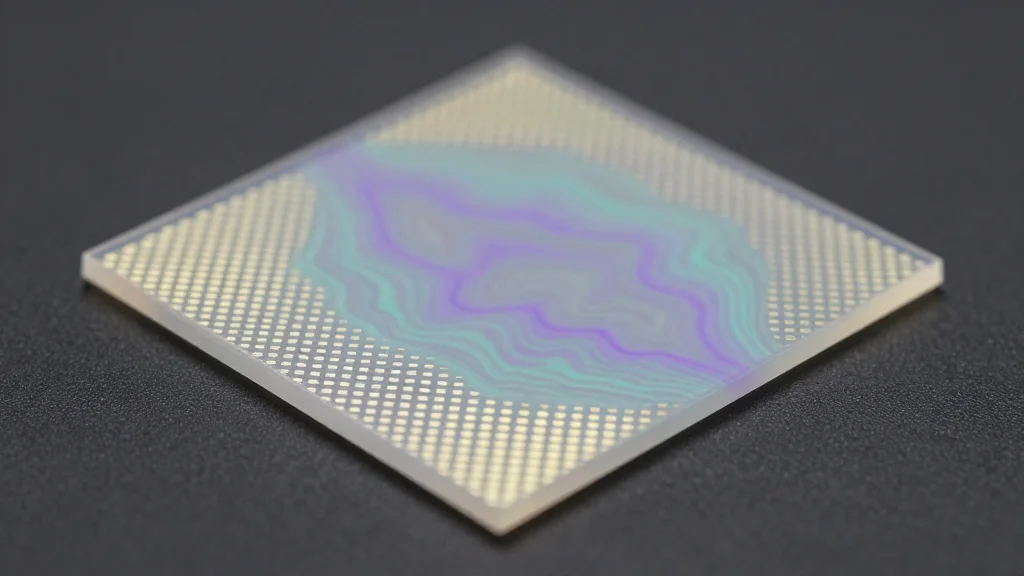
The Cornell team led by Judy Cha replaces geometric misalignment with controlled mechanical strain. By depositing lithographically patterned metal stressor films onto molybdenum disulfide (MoS₂) flakes, they generate localized biaxial or uniaxial deformation that produces deterministic moiré superlattices across the entire crystal. The strain gradient also breaks inversion symmetry, creating in‑plane electric polarization textures that can be switched with an external field. Because strain engineering is already a staple of silicon‑germanium alloying and stressed‑metal processes, the method dovetails with existing semiconductor fab lines, offering reproducibility and wafer‑scale throughput.
From a business perspective, the ability to fabricate moiré‑engineered devices using standard lithography could accelerate the commercialization of quantum‑enhanced transistors, sensors and low‑power logic. Tunable polar domains in MoS₂ promise electrically controllable resistance states, a building block for non‑volatile memory and neuromorphic circuits. Moreover, the approach lowers the entry barrier for foundries and research labs that lack specialized stacking equipment, potentially expanding the ecosystem of companies exploring twistronics. As the field matures, investors may see a surge in startups targeting strain‑based quantum platforms, reshaping the semiconductor roadmap.
Strain creates moiré 2D materials without twisting or stacking, opening more scalable route
Comments
Want to join the conversation?
Loading comments...