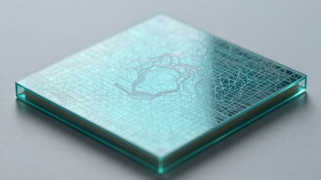
Stressed Crystal Creates Nanoscale Patterns on Chip Materials at Room Temperature
Why It Matters
The technique enables low‑cost, single‑step fabrication of photonic components on standard semiconductor materials, accelerating optoelectronic integration and reducing reliance on complex lithography.
Key Takeaways
- •Electron beam stresses alpha‑MoO₃, imprinting nanoripples on silica at room temperature.
- •Resulting wrinkles function as optical gratings for on‑chip light manipulation.
- •Process works on aluminum oxide and silicon nitride, broadening material compatibility.
- •Single‑step, chemical‑free patterning cuts cost and simplifies photonic chip manufacturing.
Pulse Analysis
Integrating light‑based functionality into silicon chips has long been hampered by the need for multi‑step lithography, high‑temperature processing, and chemically aggressive etchants. Traditional approaches such as electron‑beam lithography or nanoimprint require expensive masks and can introduce residues that degrade device performance. As the semiconductor industry pushes toward heterogeneous integration—combining electronics with photonics for data‑center and AI workloads—manufacturers are seeking scalable, low‑cost methods to embed optical elements directly onto existing dielectrics.
The Rice University breakthrough leverages the intrinsic anisotropy of alpha‑molybdenum trioxide. When an electron beam strikes the crystal, directional stress causes it to buckle, simultaneously softening the underlying amorphous dielectric. This creates a regular array of nanoripples—hundreds of nanometers across—that diffract and guide light much like a CD’s grooves. Crucially, the process occurs at ambient temperature, requires only a single exposure step, and leaves no chemical residues. By varying the crystal’s thickness or the beam’s intensity, engineers can fine‑tune ripple spacing, enabling custom optical gratings for wavelength‑division multiplexing or on‑chip interferometry.
For the photonics market, the method offers a pragmatic path to mass‑produce silicon‑based optical components without overhauling existing fabs. The ability to pattern hard insulating layers such as silica, aluminum oxide, and silicon nitride expands compatibility across the semiconductor supply chain. As data‑intensive applications demand tighter integration of lasers, modulators, and detectors, this room‑temperature, chemical‑free approach could lower capital expenditures and accelerate time‑to‑market for next‑generation optoelectronic chips. Continued research will likely focus on scaling the technique to wafer‑level throughput and exploring its synergy with emerging materials like silicon carbide and 2‑D photonic platforms.
Stressed crystal creates nanoscale patterns on chip materials at room temperature
Comments
Want to join the conversation?
Loading comments...