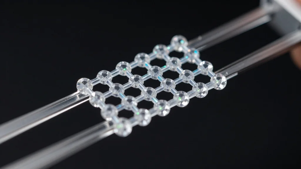
Stretching Diamond Lattice by 4% Unlocks Tunable Quantum Sensors

Why It Matters
The discovery that modest lattice strain can reconfigure SiV centers transforms diamonds from passive substrates into active, tunable quantum components. This capability bridges a gap between material science and quantum engineering, offering a scalable method to embed sensing functionality directly into the crystal lattice. For the nanotech sector, it means a new pathway to create ultra‑compact, radiation‑hard sensors that operate at room temperature, expanding the reach of quantum technologies into fields like biomedical diagnostics, structural health monitoring, and high‑pressure physics. By providing a mechanical handle on quantum properties, the work also reduces reliance on external fields or complex fabrication steps to achieve sensor calibration. This simplification could lower production costs and accelerate time‑to‑market for quantum‑enhanced devices, positioning diamond‑based platforms as a competitive alternative to silicon or superconducting technologies in emerging quantum markets.
Key Takeaways
- •SUTD and Yangzhou University demonstrated that ~4% tensile strain reconfigures SiV centers in diamond.
- •Strain induces predictable shifts in both optical emission color/brightness and magnetic spin properties.
- •The effect creates a nanoscale gauge that can measure pressure or strain via light or spin readouts.
- •Potential applications span high‑pressure research, harsh‑environment sensing, and quantum hardware calibration.
- •Future work includes experimental prototypes and extending the approach to other color centers like NV.
Pulse Analysis
The ability to mechanically tune quantum defects marks a subtle but powerful shift in how the nanotech industry approaches sensor design. Historically, diamond‑based quantum devices have been prized for their stability, but that very stability made dynamic control difficult. By introducing strain as a controllable parameter, researchers are effectively adding a new ‘knob’ to the quantum toolbox, one that can be adjusted with macroscopic actuators yet yields atomic‑scale precision. This could democratize quantum sensing, allowing smaller firms without deep expertise in laser or microwave control to develop functional devices.
From a market perspective, the finding aligns with growing demand for rugged quantum sensors in sectors such as aerospace, oil & gas, and national security. Companies that have invested heavily in diamond growth and defect engineering—like Element Six and Quantum Diamond Technologies—may see an opportunity to differentiate their product lines with strain‑engineered chips. However, the transition from computational models to manufacturable devices will require advances in strain‑application techniques, such as micro‑electromechanical systems (MEMS) or piezoelectric substrates, which could become a new competitive frontier.
Looking ahead, the broader implication is a move toward hybrid quantum‑mechanical systems where mechanical, optical, and spin degrees of freedom are co‑optimized. If the strain‑tuning concept proves viable across multiple defect types, it could catalyze a wave of multifunctional quantum components that combine sensing, communication, and processing in a single diamond chip. That convergence would not only accelerate the commercialization of quantum technologies but also reinforce diamonds’ position as a cornerstone material in the next generation of nanotech solutions.
Stretching Diamond Lattice by 4% Unlocks Tunable Quantum Sensors
Comments
Want to join the conversation?
Loading comments...