Teaching AI to Design Optical Surfaces Using Real-World Imperfections
Key Takeaways
- •ExpForm delivers 99.79% accuracy versus experimental measurements.
- •Design cycle time drops from hours to seconds, 900× faster.
- •Inverse network creates angle‑programmable spectra without new fabrication.
- •Public 25,000‑sample dataset lowers entry barrier for photonics AI.
- •Approach extends data‑driven design to visible and near‑infrared optics.
Pulse Analysis
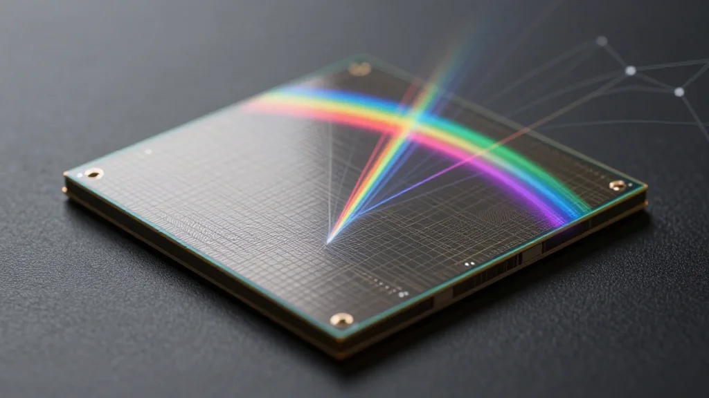
The nanophotonic community has long wrestled with the gap between idealized computer models and the messy reality of fabricated optical Fourier surfaces. These nanostructured gratings, capable of steering light into precise wavelengths and directions, are essential for compact spectrometers, augmented‑reality headsets, and high‑sensitivity sensors. Traditional design relies on finite‑difference time‑domain (FDTD) or rigorous coupled‑wave analysis, which assume perfectly smooth geometries and single‑angle illumination. In practice, surface roughness, material inhomogeneities, and angular spreads introduce discrepancies that can only be resolved through costly trial‑and‑error cycles, slowing innovation.
The SUTD team’s ExpForm framework sidesteps those limitations by training a transformer‑based neural network on 25,000 real‑world reflectance spectra collected across a broad range of incident and azimuthal angles. The forward model predicts spectral responses in milliseconds, matching experimental data with 99.79 % consistency, while the inverse model works backward to prescribe structural dimensions and illumination angles for any target spectrum. Compared with conventional FDTD, ExpForm delivers roughly a 900‑fold speedup, collapsing design loops from days to seconds. This capability unlocks angle‑programmable devices that can switch functions on‑the‑fly without re‑fabrication.
Beyond accelerating a single research project, the public release of the high‑throughput dataset lowers the barrier for other groups to develop competing or complementary AI models, fostering open benchmarking in photonics. The reality‑infused approach, already proven in the visible and near‑infrared bands, is poised to expand into high‑Q resonators, nonlinear platforms, and three‑dimensional metastructures, potentially reshaping how optical components are engineered across industries. For manufacturers of AR displays, portable spectrometers, and advanced sensing equipment, the ability to iterate designs in seconds translates into faster time‑to‑market and reduced prototyping costs, delivering a clear competitive advantage.
Teaching AI to design optical surfaces using real-world imperfections
Comments
Want to join the conversation?