The Hidden Atomic Gap that Could Break Next-Generation Computer Chips
Why It Matters
The atomic‑scale gap imposes a fundamental ceiling on how small and efficient 2D‑based transistors can become, directly affecting the roadmap for next‑generation chips. Recognizing and engineering around this limitation can save massive R&D spend and accelerate viable semiconductor breakthroughs.
Key Takeaways
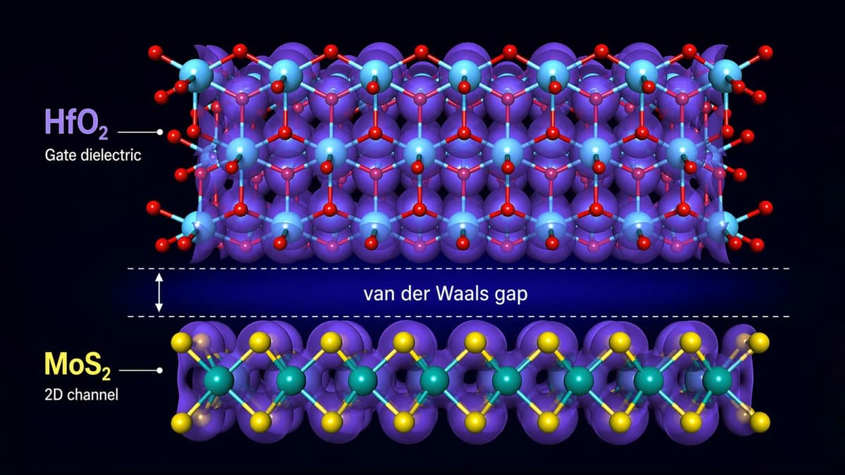
- •0.14 nm van der Waals gap weakens capacitive coupling
- •Weak interfaces can become the bottleneck for 2D chip scaling
- •"Zipper materials" create strong bonds, removing the gap
- •Industry can avoid billions in dead‑end 2D research
Pulse Analysis
The excitement around two‑dimensional materials such as graphene and molybdenum disulfide stems from their extraordinary carrier mobility and atomically thin profiles, which promise transistors far smaller than today’s silicon‑based devices. While academic studies have highlighted record‑breaking on‑state performance, they often treat the semiconductor in isolation, ignoring the insulating gate dielectric that is essential for any functional transistor. This oversight can lead to overly optimistic projections that do not translate into manufacturable products.
TU Wien’s recent work shines a light on the hidden interface problem: when a 2D channel meets an oxide dielectric, the layers are held together only by van der Waals forces, leaving a persistent 0.14‑nanometer gap. Though minuscule—smaller than a single sulfur atom—this separation dramatically reduces the electric field coupling between gate and channel, throttling the transistor’s ability to switch quickly and consume less power. As device dimensions shrink, the relative impact of this gap grows, establishing a hard physical limit that could stall the anticipated continuation of Moore’s Law for 2D‑based technologies.
A promising avenue to bypass this barrier involves "zipper materials," engineered compounds where the semiconductor and dielectric form covalent or ionic bonds, effectively stitching the layers together and eradicating the gap. By selecting material pairs that naturally interlock, designers can preserve the intrinsic advantages of 2D channels while maintaining strong capacitive control. This strategy not only safeguards billions of dollars in R&D from being sunk into infeasible approaches but also opens a clear path for the semiconductor industry to integrate 2D layers into future logic and memory nodes. Continued collaboration between materials scientists and device engineers will be crucial to map the viable material landscape and translate these insights into commercial chip production.
The hidden atomic gap that could break next-generation computer chips
Comments
Want to join the conversation?
Loading comments...