Tiny On-Chip Circuit Could Power Next-Generation Quantum and AI Technologies
Why It Matters
The breakthrough removes a key bottleneck in valleytronics, paving the way for scalable, energy‑efficient photonic processors that could accelerate quantum computing and AI workloads. Its room‑temperature operation makes commercial adoption far more realistic than many cryogenic quantum platforms.
Key Takeaways
- •Monash team created first fully integrated valleytronic chip
- •Device generates, routes, and reads light signals on a single chip
- •Operates at room temperature, easing deployment in commercial systems
- •Demonstrated simultaneous processing of two images, showing multi‑stream capability
Pulse Analysis
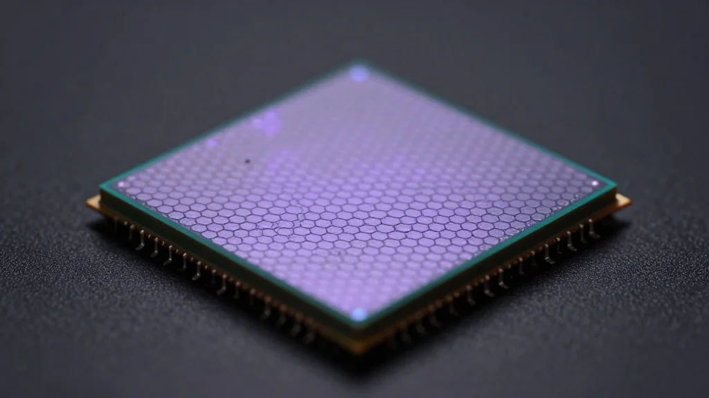
Valleytronics, the manipulation of electrons’ ‘valley’ quantum states, has long promised a new paradigm for data encoding that surpasses traditional charge‑based logic. Yet the field has been hamstrung by fragmented components—separate generators, waveguides, and detectors—requiring complex assemblies that hinder scalability. Monash University’s latest on‑chip circuit collapses these stages into a single, atom‑thin platform, marrying two‑dimensional materials with engineered metasurfaces. By doing so, it delivers precise control over light‑carried valley information, a step that could redefine how processors handle quantum‑grade signals.
The technical novelty lies in the device’s room‑temperature operation, a stark contrast to most quantum hardware that demands cryogenic cooling. Ultra‑thin semiconductors, only a few atomic layers thick, are stacked onto photonic structures without the need for direct material growth, sidestepping a major manufacturing hurdle. This simplicity not only reduces fabrication costs but also aligns the technology with existing semiconductor fabs. For AI accelerators and next‑generation quantum computers, the ability to encode, route, and read data optically on a chip promises lower power consumption and higher bandwidth, addressing two critical constraints in today’s data centers.
Beyond the lab, the collaborative nature of the project—spanning Australia, China, Singapore, Germany, and Japan—signals a global push toward integrated photonic computing. The demonstrated dual‑image processing showcases multi‑stream capability, hinting at future applications in secure optical communications, advanced imaging, and programmable photonic processors. As enterprises seek alternatives to energy‑hungry electronic chips, Monash’s valleytronic platform could become a cornerstone of the emerging photonic AI ecosystem, attracting venture capital and industrial partnerships eager to commercialize room‑temperature quantum‑grade hardware.
Tiny on-chip circuit could power next-generation quantum and AI technologies
Comments
Want to join the conversation?
Loading comments...