Tokyo Researchers Build 25‑nm Memory Chip That Improves With Size
Why It Matters
The new memory architecture directly addresses two of the semiconductor industry's most pressing challenges: power consumption and thermal management. By delivering higher performance at a smaller footprint, it could enable devices that run longer on a single charge and reduce the need for aggressive cooling solutions, which are costly and limit form factor design. Beyond consumer electronics, the technology could reshape data‑center and edge‑AI hardware, where energy efficiency translates into lower operating expenses and higher compute density. If the fabrication method proves scalable, it may also set a precedent for leveraging existing materials in novel nanostructures, accelerating innovation without the long lead times associated with entirely new material ecosystems.
Key Takeaways
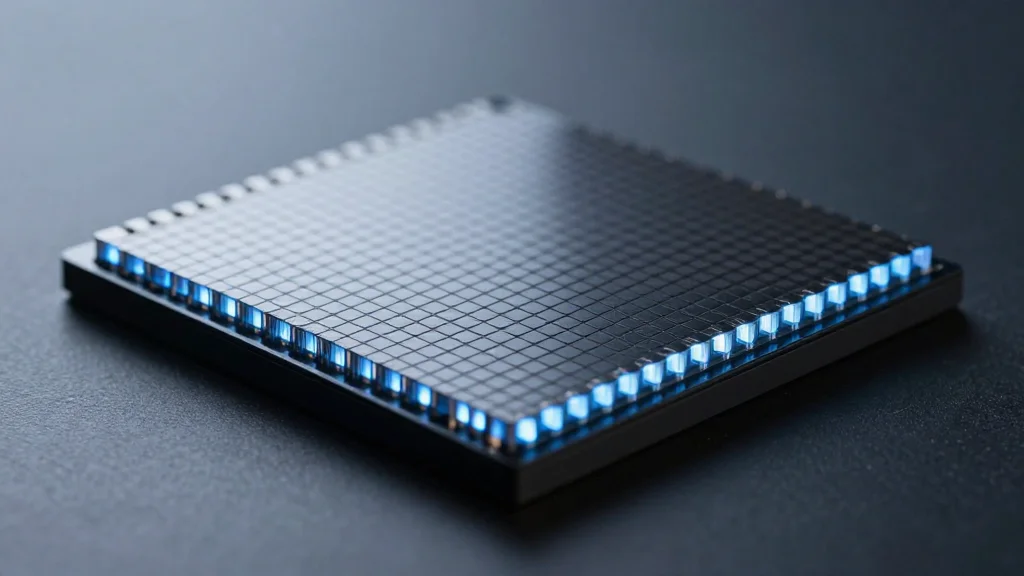
- •Memory cell size: 25 nm (≈1/3,000th hair thickness)
- •Material: hafnium oxide, already used in CMOS fabs
- •Performance improves as size shrinks, contrary to traditional scaling trends
- •Potential battery life extension: months for smartphones, weeks for wearables
- •Pilot production with a major foundry planned for late 2026
Pulse Analysis
Majima’s work underscores a shift from pure transistor scaling toward functional material engineering. The ferroelectric tunnel junction (FTJ) concept, first proposed in 1971, has long been hampered by leakage at nanometer dimensions. By turning the leakage problem on its head—making the device smaller to suppress boundary effects—the team demonstrates that clever geometry can unlock latent material properties.
Historically, each breakthrough in memory technology—DRAM, NAND flash, MRAM—has triggered a cascade of ecosystem changes, from new controller designs to revised software memory hierarchies. This 25‑nm FTJ could follow a similar trajectory if it integrates seamlessly with existing process lines. Its reliance on hafnium oxide means fabs can adopt the technique without massive capital outlays, a rare advantage in a capital‑intensive sector.
Looking ahead, the key risk lies in manufacturability at scale. Uniform electrode shaping via controlled heating must be reproducible across 300‑mm wafers, and any variability could reintroduce leakage pathways. However, if the pilot run validates the approach, the market could see a rapid rollout of low‑power memory modules, giving device makers a new lever to combat the energy ceiling that now limits both mobile and AI hardware. The competitive advantage would belong to firms that can marry this nanostructured memory with existing system‑on‑chip designs, potentially reshaping the balance of power among semiconductor giants and emerging fabless innovators.
Tokyo Researchers Build 25‑nm Memory Chip That Improves With Size
Comments
Want to join the conversation?
Loading comments...