UCLA Team Cuts Perovskite Contact Barrier Tenfold, Paving Way for Faster Chips
Why It Matters
The ability to engineer a sub‑25 nm doped region at the metal‑perovskite interface addresses a fundamental scaling obstacle that has limited perovskite devices to photovoltaic and sensor niches. By unlocking efficient charge injection, the technology opens the door to high‑frequency, low‑power logic circuits that could compete with traditional silicon in specific markets such as flexible wearables and large‑area electronics. Beyond performance gains, the method leverages inexpensive, solution‑based processing steps—thermal annealing and UV exposure—that are compatible with roll‑to‑roll manufacturing. If commercialized, this could dramatically lower the cost per transistor, accelerating the diffusion of perovskite chips into consumer and industrial products and diversifying the semiconductor ecosystem away from a single material platform.
Key Takeaways
- •UCLA researchers reduced the metal‑perovskite contact resistance region from ~250 nm to <25 nm.
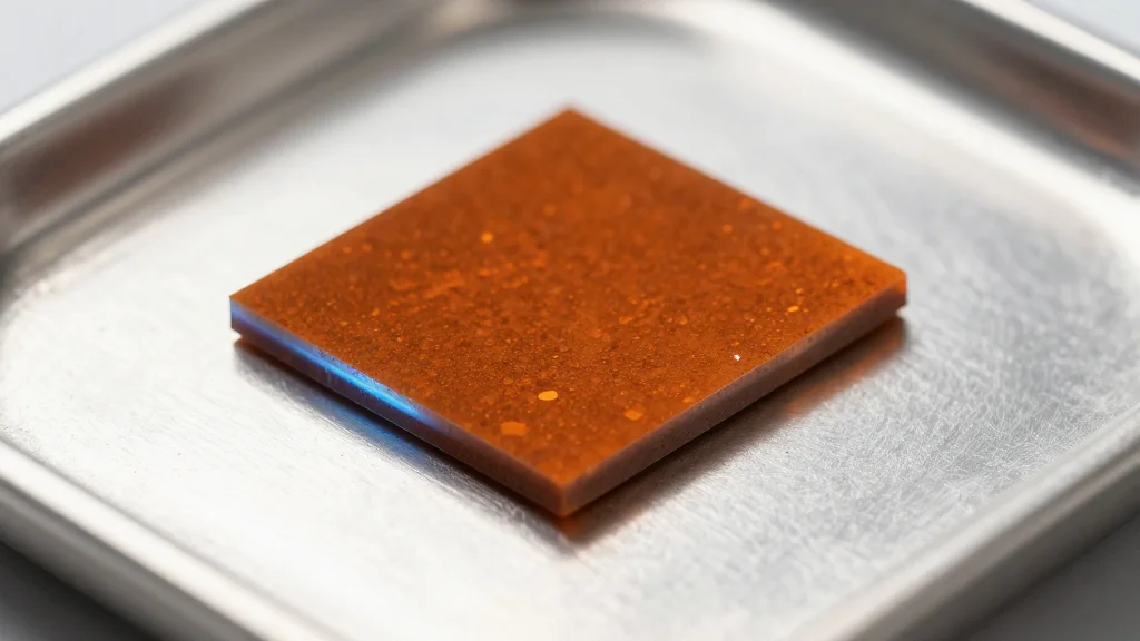
- •The technique uses silver‑oxide (Ag₂O) nanoclusters formed by mild annealing and UV exposure.
- •Localized p‑doping enables quantum tunneling, lowering operating voltage and boosting speed.
- •Published in *Nature Materials*, the work targets the scaling bottleneck that stalls perovskite electronics.
- •Prototype integration and reliability testing are planned within the next 12‑18 months.
Pulse Analysis
For decades, the semiconductor industry has chased Moore’s Law by shrinking transistor dimensions, but the metal‑semiconductor interface has become a hidden choke point as devices approach the sub‑10 nm regime. Perovskites, with their high carrier mobility and solution‑processable fabrication, promised a disruptive alternative, yet their soft lattice and susceptibility to ion migration made conventional doping untenable. UCLA’s localized charge‑transfer approach sidesteps bulk modification, delivering a nanoscale tunnel junction that mirrors the contact engineering once reserved for silicon.
From a market perspective, the breakthrough could catalyze a new class of low‑cost, high‑performance chips for applications where flexibility and large‑area coverage matter more than raw computational horsepower—think smart textiles, distributed sensor networks, and next‑generation imaging arrays. Startups already courting perovskite logic will likely view this as a de‑risking milestone, attracting fresh venture capital and prompting larger foundries to explore hybrid manufacturing lines.
However, challenges remain. Perovskite stability under prolonged electrical bias and environmental exposure is still a concern, and scaling the silver‑oxide nanocluster process from lab‑scale flakes to 300‑mm wafers will require rigorous process control. Moreover, integration with existing CMOS infrastructure will demand compatible interconnect schemes. If these hurdles are cleared, the tenfold reduction in contact resistance could translate into a comparable leap in energy efficiency, positioning perovskite electronics as a viable complement—not a replacement—to silicon in the next decade.
UCLA Team Cuts Perovskite Contact Barrier Tenfold, Paving Way for Faster Chips
Comments
Want to join the conversation?
Loading comments...