Ultrafast Dual‑Laser Technique Turns Copper Wire Into Star‑Like Plasma in Picoseconds
Why It Matters
The ability to generate and image star‑like plasma in metals within picoseconds bridges a gap between high‑energy physics and practical nanomanufacturing. Real‑time insight into ionization dynamics enables engineers to design laser‑based processes that sculpt metal at sub‑nanometer precision, potentially replacing costly lithography steps. In the broader context of fusion research, the technique offers a diagnostic tool to validate models of plasma behavior under extreme conditions, accelerating the path toward viable inertial confinement energy. Furthermore, the dual‑laser pump‑probe platform establishes a new benchmark for ultrafast measurement, encouraging investment in next‑generation XFEL facilities and high‑repetition‑rate laser systems. As industries seek faster, cleaner, and more flexible manufacturing methods, this breakthrough could become a cornerstone of the emerging nanotech economy.
Key Takeaways
- •HZDR combined an X‑ray free‑electron laser with the ReLaX optical laser on the European XFEL's HED‑HiBEF station.
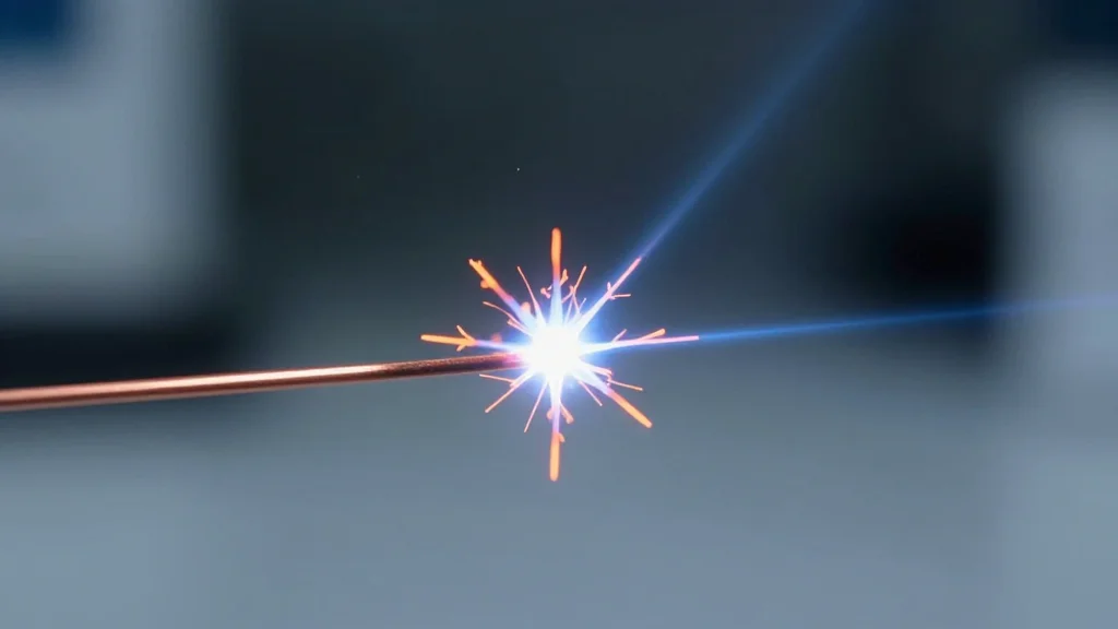
- •Laser pulses of 25 fs and 30 fs delivered ~250 trillion MW/cm², vaporizing a copper wire thinner than a human hair.
- •Pump‑probe imaging captured Cu²²⁺ ion formation peaking at 2.5 ps and recombination by ~10 ps.
- •The method provides nanometer‑scale control of metal plasma, opening pathways for ultrafast nanofabrication.
- •Future work aims to scale the technique for industrial throughput and apply it to fusion diagnostics.
Pulse Analysis
The HZDR breakthrough arrives at a moment when the nanotech sector is hungry for manufacturing methods that can keep pace with Moore's Law extensions and the rise of quantum hardware. Traditional photolithography is approaching its physical limits, and electron‑beam techniques, while precise, are too slow for high‑volume production. Ultrafast laser‑induced plasma processing, as demonstrated here, offers a complementary route that can bypass diffraction constraints entirely. By leveraging the extreme field strengths of XFELs, the process can create transient states of matter that solidify into nanostructures with unprecedented fidelity.
From a market perspective, the technology could disrupt several niches: (1) semiconductor interconnects, where copper nanowires with tailored cross‑sections are in demand; (2) photonic devices that require metallic nanogratings for plasmonic enhancement; and (3) aerospace and defense components that benefit from rapid, on‑demand repair of metal surfaces. Companies already investing in high‑repetition‑rate laser systems, such as Coherent and Light Conversion, may see a strategic advantage in integrating XFEL‑compatible diagnostics to differentiate their offerings.
Looking ahead, the main challenges will be scaling the XFEL pulse rate from the current few‑Hz regime to kilohertz levels and automating target handling to sustain industrial throughput. If these hurdles are cleared, the dual‑laser approach could become the linchpin of a new generation of nanomanufacturing plants, delivering sub‑10‑nm features in minutes rather than weeks. The ripple effect would be a faster innovation cycle for nanotech products, tighter supply chains, and a potential reduction in the carbon footprint of semiconductor fabrication.
Ultrafast Dual‑Laser Technique Turns Copper Wire into Star‑Like Plasma in Picoseconds
Comments
Want to join the conversation?
Loading comments...