Ultrasensitive X-Ray Detection Enabled by Graphene/Perovskite Heterostructures
•January 2, 2026
0
Why It Matters
The breakthrough dramatically lifts X‑ray detector performance, opening pathways for lower‑dose imaging and more reliable industrial inspection tools. It signals a viable commercial route for graphene‑perovskite hybrid sensors.
Key Takeaways
- •Graphene layer boosts carrier mobility above 10⁴ cm²/V·s
- •Sensitivity reaches 4162 µC·Gy⁻¹·cm⁻², triple prior devices
- •Detection limit drops to 9.6 nGy·s⁻¹
- •MAPbCl₃ buffer improves lattice match and adhesion
- •Device shows long‑term operational stability
Pulse Analysis
The demand for compact, high‑sensitivity X‑ray imaging has driven research beyond traditional silicon diodes toward solution‑processed semiconductors. Perovskite crystals, with their strong X‑ray absorption and tunable bandgaps, emerged as promising candidates, yet thick films often trap carriers, leading to recombination losses and unstable operation. Integrating a two‑dimensional conductor such as graphene offers a pathway to circumvent these limitations because its carrier mobility exceeds 10⁴ cm²·V⁻¹·s⁻¹, enabling rapid charge extraction. This synergy forms the basis of the latest heterostructure advances.
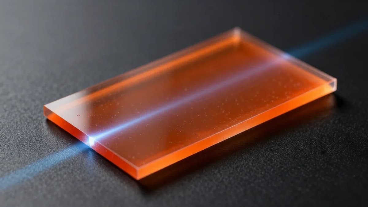
In the Dongguan University of Technology study, a graphene layer was transferred onto a CsPbBr₃ perovskite film, followed by a thin MAPbCl₃ buffer that aligns the lattice with the underlying silicon substrate. This architecture reduces interfacial defects and improves mechanical adhesion by an order of magnitude. The resulting detector delivers a sensitivity of 4162 µC·Gy⁻¹·cm⁻²—approximately three times higher than comparable perovskite‑only devices—and a detection limit of 9.6 nGy·s⁻¹. Moreover, the heterostructure maintains consistent response over extended cycling, addressing the reliability concerns that have hampered commercial adoption.
The performance leap positions graphene‑perovskite hybrids as viable contenders for medical imaging, security scanning, and industrial nondestructive testing, where low-dose, high‑resolution detection is critical. By leveraging graphene’s transport properties, manufacturers can design thinner detector stacks without sacrificing sensitivity, potentially reducing material costs and simplifying device integration. Future work will likely explore scalable roll‑to‑roll graphene transfer, alternative perovskite compositions for broader spectral response, and encapsulation strategies to further extend lifetime. As the market seeks next‑generation X‑ray sensors, this breakthrough underscores the strategic value of combining two‑dimensional materials with solution‑processed semiconductors.
Ultrasensitive X-ray detection enabled by graphene/perovskite heterostructures
0
Comments
Want to join the conversation?
Loading comments...