Visualizing Band Structures in Nanostructures: Extending Band Theory to Imperfect Periodic and Bent Systems
Why It Matters
GMBU bridges the long‑standing gap between theory and experiment for non‑periodic nanostructures, enabling rapid, accurate electronic‑structure insight that fuels material innovation in the semiconductor and spintronics markets.
Key Takeaways
- •GMBU reformulates band unfolding for finite, non‑periodic nanostructures.
- •Demonstrated on graphene, WS₂, and Bi‑Ag alloy nanoflakes.
- •Captures Dirac cones, spin‑valley coupling, and Rashba splitting on curved surfaces.
- •Enables direct comparison with high‑resolution nano‑ARPES measurements.
- •Offers a scalable framework for future nano‑electronics and spintronics design.
Pulse Analysis
Traditional band theory assumes perfect periodicity, a condition rarely met in real‑world nanomaterials such as bent nanoflakes or heterostructured islands. Without translational symmetry, conventional density‑functional calculations struggle to produce intuitive band diagrams, limiting the ability of researchers to interpret experimental spectra. The emergence of high‑resolution nano‑ARPES has heightened demand for theoretical tools that can map local electronic states onto familiar band‑structure representations, a need that GMBU directly addresses.
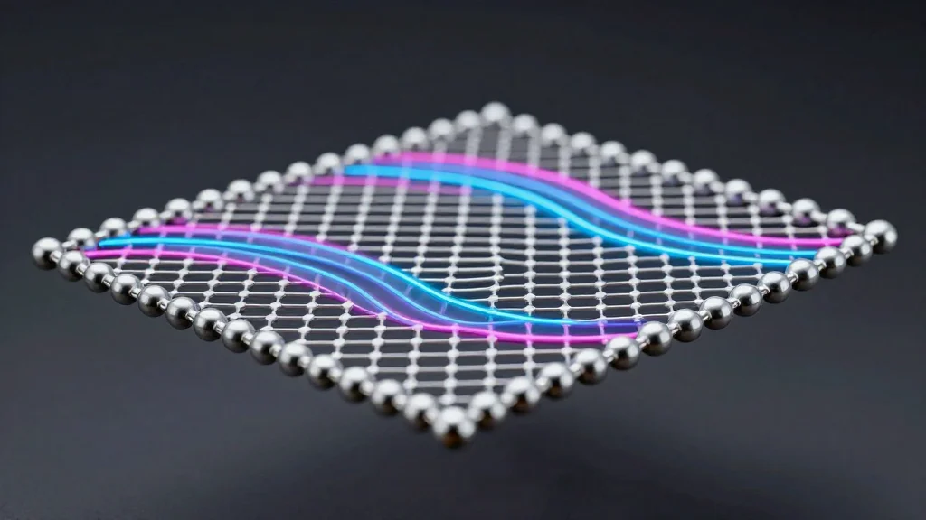
The Giant Molecule Band Unfolding (GMBU) method treats a nanostructure as a large, finite "giant molecule" and reformulates the unfolding algorithm to extract momentum‑resolved information from its wavefunctions. By applying the procedure to graphene, WS₂ and a Bi‑Ag surface alloy, the authors demonstrated clear visualization of Dirac points, spin‑valley coupling and Rashba splitting even on curved geometries. This capability confirms that local periodicity, not global symmetry, suffices for meaningful band analysis, opening a pathway to study a broad class of low‑dimensional systems previously deemed intractable.
Beyond academic insight, GMBU promises tangible industry impact. Its compatibility with existing first‑principles packages allows seamless integration into materials‑by‑design workflows, accelerating the screening of candidates for quantum‑computing, valleytronic, and spin‑orbit devices. Coupled with nano‑ARPES, the method enables rapid validation of theoretical predictions, shortening development cycles for next‑generation electronics. As nanofabrication pushes toward ever‑smaller, more complex architectures, tools like GMBU will become essential for translating nanoscale phenomena into commercial technology.
Visualizing band structures in nanostructures: Extending band theory to imperfect periodic and bent systems
Comments
Want to join the conversation?
Loading comments...