Wafer‐Scale Deterministic Fabrication of Axis‐Ratio–Engineered Silicon Nanoparticles for On‐Resonance Electric–Magnetic Dipole Interference
Why It Matters
Mass‑producing deterministic dielectric nanostructures unlocks scalable photonic components and ultra‑sensitive, label‑free biosensors, accelerating commercial adoption of nanophotonic technologies.
Key Takeaways
- •Wafer‑scale top‑down process yields Si nanoparticles with 1.7‑2.4% size variation
- •Axis‑ratio ≈2.1 aligns electric and magnetic dipoles, achieving F/B ≈12.5
- •Sensors detect refractive‑index shifts as small as 6×10⁻⁴ RIU
- •Enables label‑free monitoring of protein corona formation on single particles
Pulse Analysis
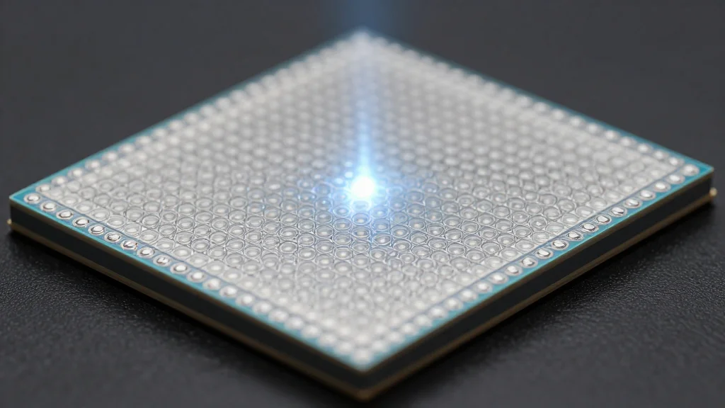
High‑index dielectric nanoparticles have reshaped nanophotonics because they support both electric and magnetic dipole resonances. When these resonances interfere constructively, the so‑called Kerker condition produces highly directional scattering, a property coveted for metasurfaces, nanoantennas, and sensing platforms. Historically, achieving the precise geometry required for on‑resonance interference relied on bottom‑up synthesis, which suffers from batch‑to‑batch variability and limited scalability, hampering integration with existing semiconductor manufacturing pipelines.
The new wafer‑scale top‑down approach leverages conventional lithography, controlled annealing, and oxidation steps to sculpt silicon pillars whose aspect ratios can be tuned deterministically. By targeting an axis‑ratio of about 2.1, the researchers aligned the electric and magnetic dipole modes, attaining a forward‑to‑backward scattering ratio of 12.5—one of the highest reported for substrate‑supported silicon nanoparticles measured under finite‑NA conditions. Uniformity across the wafer, reflected in a coefficient of variation between 1.7% and 2.4%, ensures that each particle behaves predictably, a prerequisite for reproducible device performance.
Beyond fundamental optics, the engineered nanoparticles serve as ultra‑sensitive, label‑free refractometric sensors. Their ability to resolve refractive‑index changes on the order of 10⁻⁴ RIU enables real‑time monitoring of protein‑corona formation in complex media such as serum, with sub‑nanometer spectral resolution. This capability opens pathways for point‑of‑care diagnostics, high‑throughput drug screening, and environmental monitoring. Moreover, because the fabrication is compatible with standard CMOS processes, the technology can be integrated into existing photonic chips, promising cost‑effective, mass‑produced nanophotonic sensors for the biomedical and telecommunications markets.
Wafer‐Scale Deterministic Fabrication of Axis‐Ratio–Engineered Silicon Nanoparticles for On‐Resonance Electric–Magnetic Dipole Interference
Comments
Want to join the conversation?
Loading comments...