Wafer‑Scale Oxide Dry Transfer Delivers High‑Performance MoS₂ on Flexible Substrates
Why It Matters
The oxide‑dry‑transfer method resolves the long‑standing trade‑off between scalability and material purity for 2D semiconductors. By preserving single‑crystal quality across a four‑inch wafer, the technique bridges the gap between academic prototypes and mass‑manufacturable flexible electronics, opening markets that demand both high performance and ultra‑low power consumption. Moreover, the polymer‑free process reduces post‑transfer cleaning steps, lowering production costs and improving yield, which are essential for commercial viability. In sectors such as wearable health monitoring, soft robotics, and the Internet of Things, the combination of high mobility, low subthreshold swing, and picowatt‑scale power draw enables devices that can operate continuously on harvested energy or tiny batteries. The successful integration onto a robotic gripper also hints at broader adoption in tactile sensing and AI‑edge inference, where dense, flexible sensor arrays can provide richer data streams without compromising form factor.
Key Takeaways
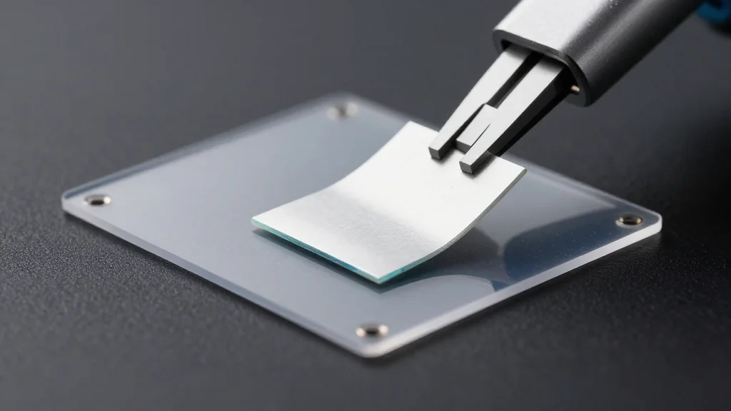
- •Wafer‑scale dry transfer of 4‑inch single‑crystal MoS₂ using a thin Al₂O₃ dielectric interlayer
- •Flexible FETs achieve 117 cm² V⁻¹ s⁻¹ electron mobility, 68.8 mV dec⁻¹ subthreshold swing, and 10¹² on/off ratio
- •Inverter circuits on flexible substrates reach a voltage gain of 218 with 1.4 pW µm⁻¹ power consumption
- •Active‑matrix tactile sensor integrated onto a robotic gripper demonstrates real‑time pressure mapping
- •Polymer‑free process eliminates contamination, paving the way for roll‑to‑roll manufacturing of 2D‑material devices
Pulse Analysis
The oxide‑dry‑transfer breakthrough arrives at a pivotal moment for the flexible electronics ecosystem. Historically, the promise of 2D transition‑metal dichalcogenides has been hampered by the inability to move large‑area crystals without degrading their electronic quality. Wet‑transfer methods, while scalable, introduce polymer residues that scatter carriers and raise threshold voltages, eroding the very advantages that make MoS₂ attractive. By inserting a high‑κ Al₂O₃ layer, the new process creates a chemically inert bridge that both adheres the crystal and serves as a gate dielectric, effectively killing two birds with one stone. This dual function reduces process steps, cuts material waste, and aligns with existing thin‑film deposition tools used in display manufacturing.
From a market perspective, the ability to produce wafer‑scale, high‑performance MoS₂ on flexible substrates could catalyze a shift away from amorphous oxide semiconductors that dominate current flexible displays. While amorphous oxides offer decent mobility, they fall short of the 100 cm² V⁻¹ s⁻¹ threshold needed for high‑speed logic and advanced sensor arrays. The reported 117 cm² V⁻¹ s⁻¹ mobility places MoS₂ comfortably above that line, suggesting that future flexible processors could rival their rigid silicon counterparts in speed while retaining bendability. Companies that have invested heavily in polymer‑based transfer equipment may need to pivot, either by licensing the oxide‑dry‑transfer technology or by developing competing contamination‑free approaches.
Looking ahead, the next challenge will be integrating this transfer method with large‑area deposition of other 2D materials, such as graphene for interconnects or h‑BN for encapsulation. A heterogeneous stack that combines the best of each material could unlock truly multifunctional flexible systems—high‑speed logic, transparent conductors, and robust passivation—all fabricated in a single, roll‑to‑roll line. The current work provides a template for that vision, and its impact will likely be measured not just in device metrics but in how quickly the supply chain adapts to a new manufacturing paradigm.
Wafer‑Scale Oxide Dry Transfer Delivers High‑Performance MoS₂ on Flexible Substrates
Comments
Want to join the conversation?
Loading comments...