Weak‐Interaction‐Driven Self‐Positioning for Multi‐Site Modification in Perovskite Solar Cells
•February 2, 2026
0
Companies Mentioned
Why It Matters
The approach dramatically simplifies interfacial engineering, unlocking near‑theoretical efficiencies while easing manufacturing complexity for scalable perovskite photovoltaics.
Key Takeaways
- •Self-positioning modifies perovskite interfaces without extra steps
- •Weak interactions drive alkali ion migration to SnO2 interface
- •Li2Pc yields 1.204 V VOC and 25.60% efficiency
- •VOC reaches 95% of theoretical limit
- •Scalable 1 cm² devices achieve 1.177 V VOC
Pulse Analysis
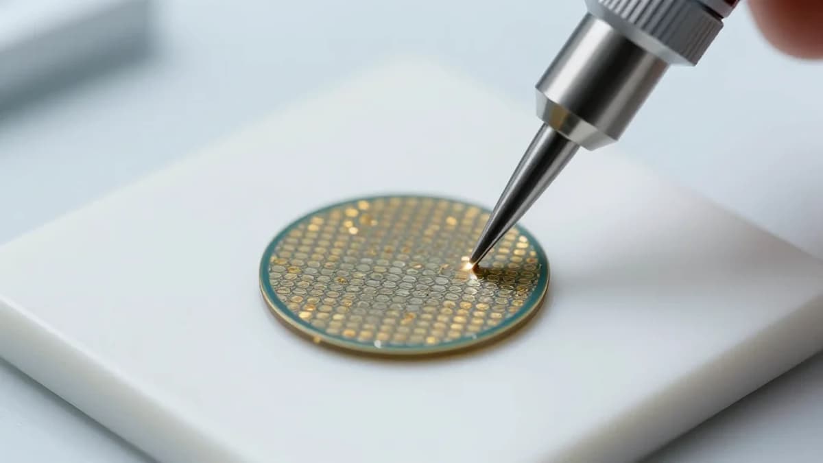
Perovskite solar cells have surged toward the efficiency frontier, yet non‑radiative recombination at multiple interfaces remains a bottleneck. Traditional interfacial engineering relies on sequential ultrathin layers, demanding precise deposition control and adding cost. By targeting the fundamental chemistry of modifier‑perovskite interactions, the new self‑positioning method sidesteps these hurdles, offering a chemically driven route to align energy levels and passivate defects across the bulk, surface, and transport layers simultaneously.
The core of the technique lies in metal phthalocyanine compounds whose ligands exhibit weak coordination with alkali metals. During spin‑coating, these complexes dissociate; alkali ions such as Li⁺ or Na⁺ preferentially migrate toward the SnO₂/perovskite junction, while the organic ligands accumulate at the film’s top surface. This dual‑site redistribution creates a stronger built‑in electric field and curtails trap‑assisted recombination without any post‑deposition treatment. The result is a record‑setting open‑circuit voltage of 1.204 V and a power conversion efficiency of 25.60%, pushing the device to 95% of its thermodynamic VOC ceiling.
Beyond performance, the self‑positioning strategy holds commercial promise. Eliminating extra coating steps reduces processing time and equipment wear, facilitating roll‑to‑roll manufacturing and larger‑area modules. The demonstrated 1 cm² devices retain high VOC, indicating that the chemistry scales without degradation. As the photovoltaic market seeks cost‑effective, high‑efficiency alternatives to silicon, such intrinsically simple yet powerful interfacial designs could accelerate perovskite adoption and drive further research into tunable weak‑interaction modifiers.
Weak‐Interaction‐Driven Self‐Positioning for Multi‐Site Modification in Perovskite Solar Cells
0
Comments
Want to join the conversation?
Loading comments...