World‑First Spintronic P‑Bit on Silicon Chip Demonstrated by Japan‑U.S. Team
Companies Mentioned
Why It Matters
The demonstration of a spintronic p‑bit on a silicon substrate bridges a critical gap between exotic nanomagnetic research and mainstream semiconductor manufacturing. By using a 130‑nm CMOS process, the work shows that probabilistic computing can be pursued without the need for entirely new fab lines, reducing capital expenditures for chipmakers. For AI hardware, the ability to perform massive parallel sampling with minimal energy could reshape the economics of inference at the edge, where battery life and thermal constraints dominate design choices. Moreover, the collaboration between a leading Japanese university and a U.S. standards institute underscores the global nature of next‑generation computing research. Successful scaling could spur new industry consortia, attract venture funding, and influence roadmaps of major foundries that are already investing in spintronic and magnetic‑memory technologies.
Key Takeaways
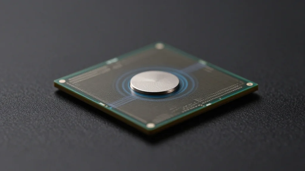
- •World‑first integrated spintronic p‑bit fabricated on silicon using 130‑nm CMOS.
- •Joint effort by Tohoku University (Japan) and NIST (U.S.) published in IEEE Electron Device Letters.
- •Demonstrated stochastic voltage fluctuations and voltage‑controlled averaging, essential for probabilistic computing.
- •Spintronic p‑bits promise low‑power AI inference by exploiting intrinsic magnetic randomness.
- •Next milestones include scaling to multi‑p‑bit arrays and benchmarking against conventional AI accelerators.
Pulse Analysis
The spintronic p‑bit prototype arrives at a moment when the semiconductor industry is grappling with the limits of Moore's Law and the soaring power demands of AI workloads. Traditional GPUs and tensor‑processing units (TPUs) have delivered performance gains but at the cost of escalating energy consumption. Probabilistic computing, and specifically spintronic implementations, offer a fundamentally different paradigm: instead of deterministic logic, they harness randomness to explore solution spaces more efficiently. This could translate into a new class of AI accelerators that are both faster and greener.
Historically, spintronic technologies have been championed for non‑volatile memory (e.g., MRAM) but have struggled to find a clear compute niche. The integration of p‑bits directly into a CMOS‑compatible process changes that narrative, positioning spintronics as a viable compute substrate rather than a peripheral memory element. If the research team can demonstrate reliable operation across large arrays, they may unlock a competitive edge against emerging alternatives such as neuromorphic chips and photonic AI processors, which also aim to reduce energy per operation but require distinct manufacturing ecosystems.
From a market perspective, the ability to produce spintronic p‑bits in existing fabs could attract early adopters in sectors where power is at a premium—autonomous vehicles, IoT edge nodes, and satellite computing. Venture capital is already flowing into spintronic startups, and a successful scaling path could accelerate funding cycles and spur partnerships with major foundries like TSMC and GlobalFoundries. However, challenges remain: ensuring device uniformity, managing thermal stability, and developing software stacks that can translate AI models into probabilistic algorithms. The next 12‑18 months will be decisive as the research moves from single‑device proof‑of‑concept to system‑level demonstrations that can be benchmarked against established AI hardware.
World‑First Spintronic p‑Bit on Silicon Chip Demonstrated by Japan‑U.S. Team
Comments
Want to join the conversation?
Loading comments...