
Below the Surface: From Substrate to System—Why Integration Is the Real RF Breakthrough
Chandra Gupta argues that the true breakthrough in RF engineering lies not in the ceramic substrate alone but in the seamless integration of substrate, package, and module. Modern RF packages are treated as electrical elements, with engineered transitions that preserve impedance and minimize loss. Integrated ceramic modules combine amplifiers, filters and matching networks on a shared platform, cutting interconnects, improving thermal paths, and boosting reliability. This systems‑thinking approach accelerates time‑to‑market for 5G, radar and other high‑frequency applications.

CG Semi Included in Newly Approved Semiconductor SEZs
The Indian government has approved a special economic zone (SEZ) in Dholera, Gujarat, for Tata Semiconductor Manufacturing’s chip‑fabrication plant, covering 66.16 hectares. Tata plans to invest roughly ₹91,000 crore (about $11 billion), positioning the project as the country’s first large‑scale semiconductor fab....
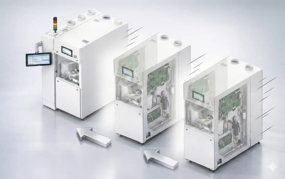
PacTech Launches Scalable Modular Wet-Bench System for Advanced Semiconductor Packaging
PacTech announced a new Modular Wet‑Bench System that offers a compact, scalable solution for semiconductor wet processing. The base module occupies a 1850 × 1500 mm footprint and houses two 8‑inch tanks, with optional robotic arms for semi‑automated handling. Designed for both R&D...

Intel Foundry Achieves Breakthrough with World’s Thinnest GaN Chiplet Technology
Intel Foundry unveiled the world’s thinnest gallium‑nitride (GaN) chiplet, featuring a 19 µm silicon base harvested from a 300 mm GaN‑on‑silicon wafer. The chiplet integrates GaN power transistors with silicon digital logic on a single die, eliminating the need for separate companion...

Advanced iBGA Image Sensor Encapsulation
DELO introduced a PFAS‑free encapsulation material designed for automotive image sensors used in advanced driver‑assistance and autonomous systems. The formulation delivers low warpage, fine‑pitch flow control, and automotive‑grade reliability, addressing the harsh temperature, vibration, and moisture conditions of vehicle environments....
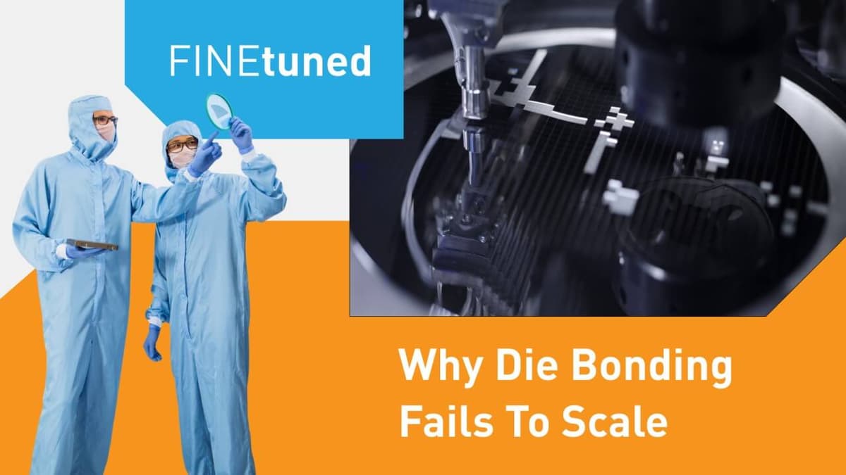
Why Die Bonding Fails to Scale: How Do You Move From Prototype to Production Without Starting Over?
Die‑bonding processes often succeed in the lab but falter when moved to high‑volume production because the R&D setup differs from the manufacturing environment. The article argues that the root cause is a lack of production‑centric validation, leading to yield loss,...
Indium Corporation Announces Strategic Agreement for Domestic Critical Metals Recovery
Indium Corporation has signed a long‑term offtake framework with Flash Metals USA, a Metallium subsidiary, to purchase critical metals recovered from electronic scrap using Flash Joule Heating technology. The agreement covers gallium, germanium, copper, tin, gold and indium, with an...
The Silicon Desert
The Silicon Desert map visualizes Arizona’s rapidly expanding technology ecosystem, covering semiconductor, hardware, software, AI, IoT, and life‑science sectors. It lists more than 50 participants, from early‑stage startups to Fortune 100 multinationals such as Intel, IBM, and Boeing. The Arizona Technology...