Why Die Bonding Fails to Scale: How Do You Move From Prototype to Production Without Starting Over?
Why It Matters
Aligning die‑bonding development with production directly impacts time‑to‑market, cost efficiency, and revenue for advanced‑packaging firms, making scalability a competitive differentiator.
Key Takeaways
- •Transfer gaps cause yield drops in volume production
- •Unified hardware/software eases prototype-to-production transition
- •Process recipes must be reproducible across systems
- •High-mix environments need flexible bonding platforms
- •Early production alignment cuts development cycles
Pulse Analysis
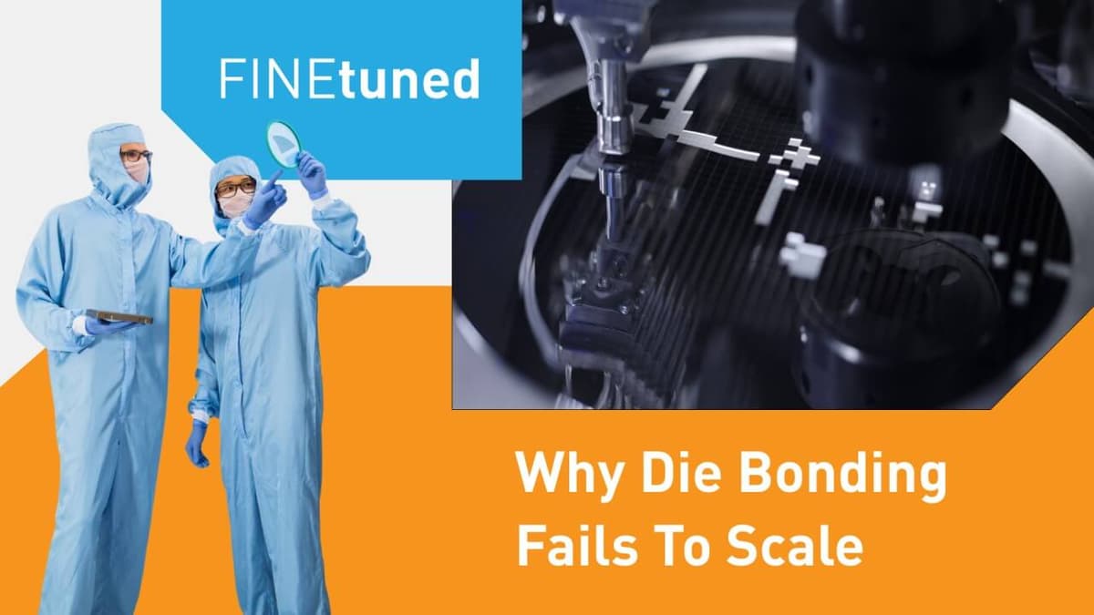
Advanced packaging relies on precise die‑bonding to attach components such as lasers, photonic chips, and IR sensors. While R&D labs can achieve sub‑micron alignment with specialized bonder models, the moment a design moves to a production line, variations in equipment, software, and thermal environments introduce drift. This drift erodes yields, inflates scrap rates, and forces costly re‑qualification, especially as manufacturers juggle diverse device families—from silicon photonics transceivers to SiC power modules. The core issue isn’t the bonding chemistry but the disconnect between prototype and production ecosystems.
A proven remedy is to standardize the entire bonding workflow from day one. Selecting an R&D bonder that mirrors the production platform ensures that hardware tolerances, control algorithms, and recipe parameters remain consistent. When the same software stack and process logic are used, the transition becomes a scale‑up rather than a redesign. Real‑world examples, such as IR sensor flip‑chip assembly, demonstrate that storing alignment and temperature profiles as immutable recipes enables seamless replication on high‑throughput lines, preserving performance while boosting throughput.
Strategically, companies that embed production considerations early gain a decisive market edge. Shorter development cycles translate to faster customer deliveries and lower capital exposure. Moreover, a unified ecosystem supports high‑mix, low‑volume production—a growing demand driven by AI, LiDAR, and micro‑LED applications. Vendors like Finetech are responding with next‑generation, high‑mix die‑bonders designed for this very continuity, promising reduced variation and faster learning loops. Organizations that adopt this approach can expect stabilized yields, predictable cost structures, and stronger competitive positioning in the fast‑evolving semiconductor landscape.
Why Die Bonding Fails to Scale: How Do You Move from Prototype to Production Without Starting Over?
Comments
Want to join the conversation?
Loading comments...