
UCIe Vs. BoW: Practical Insights For Choosing The Right Chiplet Standards
The white paper compares Universal Chiplet Interconnect Express (UCIe) and Bunch of Wires (BoW) as the two leading die‑to‑die interconnect standards for chiplet architectures. It outlines how UCIe emphasizes a standardized, interoperable ecosystem while BoW focuses on simple, flexible wiring. A channel‑level case study evaluates signal‑integrity metrics such as eye diagrams, VTF loss, and crosstalk, finding UCIe provides clearer compliance guidance. The document also highlights the role of advanced EDA tools in early validation to lower design risk.
Creating A Moore’s Law For AI Scaling
The semiconductor industry is confronting a looming AI scalability crisis, as next‑generation agentic and physical AI systems could demand up to 150× the compute of today’s large language models. Leaders such as imec, Samsung, TSMC and AMD argue that a...
Tool-Assisted LLM Targets RTL Code Generation (UC Riverside, Futurewei)
Researchers from UC Riverside and Futurewei introduced LLM4RTL, a tool‑assisted large language model system for generating RTL code. The team created a "judge‑renew‑check‑renew‑check" (JRCRC) pipeline that iteratively refines public Verilog datasets using a hierarchy of commercial LLMs, producing higher‑quality training...
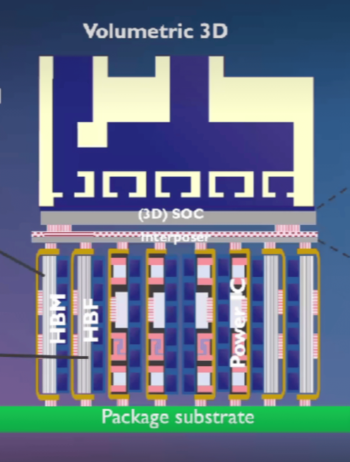
How To Build Billions of Bumps
Hybrid bonding with a 1 µm pad pitch can pack roughly 1,000 connections per millimeter, allowing a single package to host tens of billions of interconnects. Achieving such density demands wafer‑scale uniformity, sub‑nanometer surface roughness, and precise copper CMP to avoid...
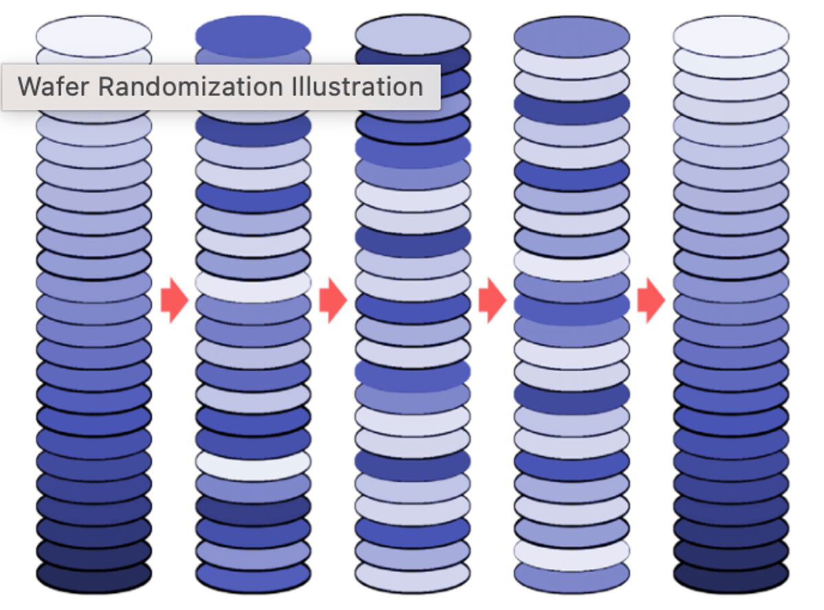
Randomizing Wafers To Zero In On Process Problems Much Faster
Wafer randomization, combined with slot‑positional analysis, enables fabs to pinpoint defect origins far more quickly than traditional methods. Historically, achieving randomization required costly sorters, specialized software, and added labor, often slowing cycle time. By automatically randomizing wafers and tracking each...

Making On-Chip Photonics Manufacturable
Leading AI‑driven data centers are hitting system‑level bandwidth and energy limits, prompting chipmakers to embed silicon photonics directly into packages and eventually onto chips. While the physics of moving optical engines closer to ASICs promises lower power and higher speed,...

Blog Review: June 17
The June 17 Semiconductor Engineering blog roundup spotlights a wave of technical breakthroughs across storage, AI, photonics, and high‑performance computing. Cadence’s Controller Memory Buffer (CMB) opens on‑chip memory to hosts, slashing NVMe latency, while Siemens demonstrates a BusFrequencyMultiplier/Divider pair that doubles...

Modeling Multi-GPU Traffic For Distributed AI Workloads (UW Madison, AMD)
Researchers from the University of Wisconsin‑Madison and AMD unveiled Eidola, a scalable extension to the gem5 simulator that models inter‑GPU communication traffic in distributed AI workloads. The tool uses a lightweight “eidolon” GPU model and cycle‑level timing profiles to emulate...

Physical Neural Networks: A Survey (U. Of Lübeck, TU Hamburg)
Researchers from the University of Lübeck and TU Hamburg released a comprehensive survey titled “Beyond Silicon: Materials, Mechanisms, and Methods for Physical Neural Computing.” The paper catalogs non‑silicon substrates—including memristors, photonic circuits, mechanical metamaterials, microfluidic networks, chemical reactors, and living...

Research Bits: June 15
Researchers at Georgia Tech and Penn State unveiled a ferroelectric NAND flash memory that endures radiation levels up to one million rads—about 30 times the tolerance of conventional NAND—making it suitable for deep‑space missions. In parallel, Polytechnique Montréal demonstrated a...

Optimizing EUV Source Efficiency With Radiation-Hydrodynamic Simulations (U. Of Osaka Et Al.)
Researchers from Osaka University and partner institutes used the STAR-1D radiation‑hydrodynamics code to simulate over 140,000 laser‑parameter combinations for tin‑plasma extreme ultraviolet (EUV) sources. The study identified a global conversion‑efficiency maximum of 5.63 % at a 5.5 µm driver wavelength, and a...

Building A Production-Ready Optically Connected Rack For AI Scale-Up
AI workloads are pushing rack‑scale systems beyond the limits of copper interconnects, prompting a shift to co‑packaged optics (CPO). Ayar Labs and Wiwynn announced a partnership to build a production‑ready, optically connected rack that integrates CPO, liquid cooling, high‑voltage DC...

Cloud HPC For AI: Addressing Latency, Cost, And Scale At The Architectural Level
Moving high‑performance computing (HPC) workloads to the cloud is no longer a simple lift‑and‑shift exercise. To keep AI training efficient, organizations must redesign architectures to cut latency, improve utilization, and enable predictable scaling. Hybrid models that keep latency‑critical tasks on‑premises...

Re-Architecting Die-to-Die IO For AI
Synopsys unveiled its 3DIO solution IP, a fully digital die‑to‑die I/O architecture designed for hybrid‑bonded 3D stacks. The PHY supports 4‑6 Gb/s per link at under 0.05 pJ/bit and scales through a cluster‑based design with built‑in redundancy and BIST. By eliminating analog...

Beyond The Demo: Deploying And Evaluating Open-Source AI Workloads
The article highlights how developers are moving beyond simple demo runs to reproducible edge‑AI deployment using the CIX Armv9 platform and open‑source toolchains. It showcases two learning paths—Mixture‑of‑Experts (MoE) large‑language models and multimodal inference—to illustrate systematic evaluation of memory, routing,...