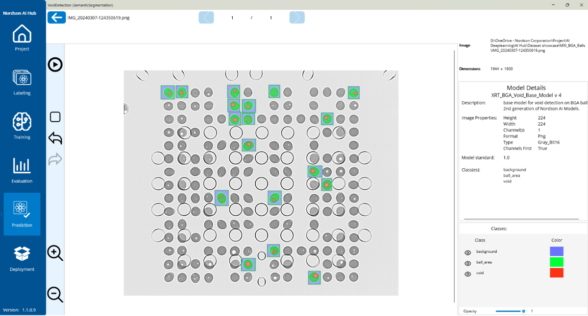
AI Models Transform Defect Inspection And Review, But Can Fail To Scale
AI-driven defect inspection is rapidly improving yield by capturing more defect types and separating real defects from nuisance ones. New deep‑learning models can identify hard‑to‑see wafer‑edge defects in hybrid‑bonded chips, a task where traditional algorithms fall short. However, scaling these models beyond pilot projects remains difficult, with more than 70% of initiatives stalling due to data fragmentation and legacy infrastructure. Experts stress that robust data integration, synthetic‑data generation, and enterprise‑grade AI platforms are essential for broader deployment.

Effective UX/UI Is A Critical Link Between AI Insights And Yield Improvement
The semiconductor sector is recognizing that AI’s true value hinges on the usability of its interfaces. As advanced nodes and heterogeneous integration increase process variability, engineers need transparent, real‑time UX/UI that surfaces confidence metrics, data lineage, and multi‑path recommendations. Modern...
Why Analog And Mixed-Signal Chips Resist Adaptive Test
Analog and mixed‑signal (A/MS) testing has long relied on specification‑based methods, but the new IEEE 2427‑2025 standard now provides a framework to quantify defect coverage for the first time. The standard helps engineers distinguish true silicon defects from normal process...

Research Bits: June 8
Researchers at POSTECH unveiled a ZnO‑Te heterojunction transistor that exhibits double negative differential transconductance, enabling a single device to act as a frequency quadrupler and quadruple data‑processing speed. In parallel, Tohoku University and NIST integrated a spintronic probabilistic bit (p‑bit)...

Orbital Data Centers Are Souped-Up Satellites – For Now
Companies such as SpaceX, Blue Origin and Nvidia are pursuing orbital data centers—essentially compute‑heavy satellites—to deliver up to 100 GW of AI processing power by deploying millions of units. The concept relies on sun‑synchronous solar power, but engineers face steep hurdles...

Keeping Security Algorithms Current Is Getting Harder
Security algorithms are now a lifecycle issue that spans chip design, manufacturing, deployment, and long‑term maintenance across fragmented supply chains. Hardware must be built with cryptographic agility, secure roots of trust, and reliable update mechanisms to counter emerging threats, especially...

Securing Terabit Ethernet For AI: Where MACsec, IPsec, And UET TSS Each Fit (And Why You Need More Than One)
As AI and HPC workloads push Ethernet speeds beyond 1 Tbps, securing the fabric requires more than a single protocol. The article explains how MACsec, IPsec, and the new Ultra Ethernet Transport Security Sublayer (UET‑TSS) each protect different layers—link, network, and...
Beyond PCIe Compliance: Why Stress Testing Is Crucial For Edge AI Deployments
PCIe compliance alone isn’t enough for edge AI deployments. While compliance confirms specification conformance under lab conditions, it doesn’t reveal how much performance margin remains when devices face thermal stress, power‑state cycling, and bursty inference traffic. Stress testing extends validation...

Defending Smart Homes Against AI Cyber Attacks
Large language models such as Claude Mythos and GPT‑5.5 now possess cybersecurity skills comparable to seasoned professionals, and open‑weight variants can achieve similar results. This emerging capability lets attackers rapidly discover and exploit firmware bugs in smart‑home devices, while the...

The Edge LLM Offload Story
Developers seeking on‑device large language models now have a dedicated solution as Synaptics and Google Research combine the Astra SL2610 processor with the Coral NPU to form the Torq NPU. The platform tackles edge‑LLM bottlenecks through static model conversion, hardware‑accelerated...
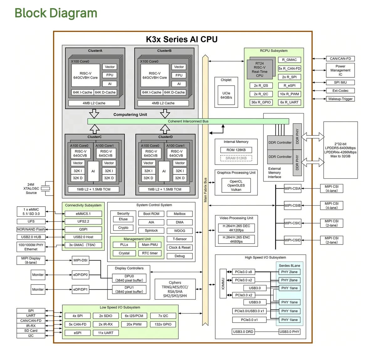
RISC-V And GPU Synergy In Practice: A Path Towards High-Performance SoCs
SpacemiT’s newly launched K3 processor showcases how RISC‑V CPUs can serve as the backbone of high‑performance system‑on‑chips. The chip runs up to 2.4 GHz on in‑house X100 cores, delivering roughly 130 K DMIPS, and bundles 60 TOPS INT4 AI compute capable of handling...

Using Graph Attention for Virtual Metrology in Semiconductor Manufacturing (Intel Foundry, ASU)
Researchers from Arizona State University and Intel Foundry introduced a graph attention‑based virtual metrology (VM) framework to predict film thickness in semiconductor deposition processes. The model treats each step‑parameter pair as a graph node, learns temporal embeddings from high‑frequency sensor...

Scaling Open-Source HW Accelerator for Deep NN Inference (UDE, Fraunhofer IMS)
Researchers at the University of Duisburg‑Essen and Fraunhofer IMS unveiled OpenEye, an open‑source, sparsity‑aware FPGA accelerator for deep‑neural‑network inference. The architecture is built from configurable clusters of processing elements that stream data and can be scaled to match performance or...

Research Bits: Jun. 2
Researchers at Monash University unveiled an integrated valleytronics circuit that can generate, route, and read light‑based information on a single chip at room temperature, simultaneously handling multiple data streams and demonstrating dual‑image encoding. At the University of Texas at Austin,...

The Sub-2nm Paradox
The semiconductor industry is confronting a paradox at sub‑2nm nodes: while transistor density continues to rise, process variation, RC delay, and SRAM scaling limits are driving yields down and costs up. Foundries are extending node roadmaps to 10 angstrom (≈1 nm) and...

Building Fixed HW Implementations of Neural Networks (Yale, Cornell Et Al.)
Researchers from Yale, Cornell, Boston University and NTT Research propose Physical Foundation Models—fixed hardware implementations of large‑scale neural networks. By embedding trillion‑parameter models directly into the physical substrate, such as 3D nanostructured glass, they claim orders‑of‑magnitude gains in energy efficiency,...

Chip Industry Week In Review
The ECTC conference highlighted a wave of advanced‑packaging breakthroughs, including ASE’s automated 310 mm × 310 mm panel‑level line slated for 2027, Imec and EV Group’s 200 nm wafer‑to‑wafer hybrid bonding, and SK hynix’s cooling‑integrated HBM interface that cuts thermal resistance by 30%. Parallel announcements underscored...

From Billions Of Violations To Actionable Insights: Calibre Vision AI
Calibre Vision AI, launched by Siemens in 2025 and upgraded in 2026, provides AI‑guided, instance‑complete triage of full‑chip DRC results at advanced nodes. The platform now supports real‑time incremental loading of OASIS data, persistent workflow states, and tighter integration with...

Swapping Out Chiplets: I/Os Vs. Compute
Chiplet‑based architectures let designers replace compute, memory, or I/O dies independently, preserving stable blocks while adopting newer process nodes or faster protocols. Companies often keep I/O dies on mature nodes and upgrade compute chips from 5 nm to 3 nm for power...

Observability Is Essential For Modern Silicon
Industry leaders highlighted that on‑die observability is becoming essential for modern silicon, especially as designs shift toward chiplet‑based, heterogeneous systems. Visibility into power, temperature, and inter‑die communication enables real‑time optimization, reliability debugging, and security monitoring across automotive, aerospace, and data‑center...

Using SystemC TLM Modeling To Solve AI Data Movement Challenges
AI silicon performance hinges on data arriving at the right rate and latency, not just raw compute power. Early in a design, engineers must explore how real AI workloads move through the network‑on‑chip (NoC) to spot bottlenecks. SystemC transaction‑level modeling...

Foundation Model For Physics: The Next Layer Of Intelligence For Engineering
Foundation models are extending beyond language and vision to physics, aiming to provide deterministic, solver‑grounded reasoning across engineering designs. Unlike traditional episodic simulations, a physics foundation model would generalize across geometries, materials, and boundary conditions without retraining for each case....

Wafer-Scale Vs. Chiplets: The New War? Part 1
Cerebras’ recent IPO highlights a shift in semiconductor strategy as the company scales an entire wafer into a single compute engine, the Wafer‑Scale Engine (WSE‑3). By treating the wafer as one chip, Cerebras has pioneered solutions for yield mapping, distributed...

The Shape Of Prompts: Exploring Their Effect On Inference Infrastructure
The article introduces Keysight’s AI Inference Builder, a workload‑morphology engine that models the "shape" of AI prompts across compute, memory, and latency dimensions. By visualizing prompts as vectors on spider charts, it shows how prefill‑heavy, decode‑heavy, and memory‑heavy workloads stress...

Deterministic, Solver-Accurate Thermal and Warpage Analysis at Manufacturing Resolution for Advanced 2.5D HBM Packages
Thermal management has become the primary bottleneck for high‑performance computing and AI accelerator packages that stack multiple High Bandwidth Memory (HBM) dies on a silicon interposer. Modern 2.5D designs can exceed 1 kW of thermal design power, creating intense die‑to‑die crosstalk...

Characterization of GPU-Based Inference for Reasoning-Centric LLMs (Micron, Argonne)
Researchers from Micron and Argonne released a paper characterizing GPU inference for reasoning‑centric large language models. They show that chain‑of‑thought workloads shift inference into a capacity‑bound regime, where KV‑cache fragmentation curtails data parallelism. Tensor parallelism unlocks stranded memory and delivers...

Detecting Defect-Induced Silent Data Corruptions in CPUs (Stanford, Google)
Stanford and Google researchers introduced ITHICA, an intra‑thread instruction‑checking framework that uncovers defect‑induced silent data corruptions (SDCs) in CPUs. The method challenges the long‑standing assumption that silicon defects produce consistent errors, showing that identical instructions can yield divergent results depending...

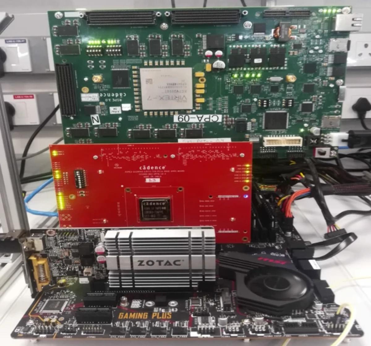
An Agent-Driven End-to-End HW-SW Co-Design Benchmark for Heterogeneous SoCs (Columbia, IBM)
Columbia University and IBM Research introduced HSCO-Bench, the first benchmark that tests large language model (LLM) agents on end‑to‑end hardware‑software co‑design for heterogeneous system‑on‑chips. The suite runs on an open‑source SoC platform and deploys generated designs to an AMD Virtex‑7...
Advancing Heterogeneous Integration Through Industry Roadmap Improvements
A multinational research team led by Intel published a perspective in Nature Reviews Electrical Engineering calling for a new generation of heterogeneous integration (HI) roadmaps. The paper argues that existing roadmaps lag behind rapid advances in AI, 5G/6G, and aerospace,...

AI & Energy: Bending The Curve
Artificial intelligence is expanding at a pace that forces data‑center power consumption to rise 4–5 times each year, pushing installations toward megawatt and eventually gigawatt scales. This surge strains grid capacity and makes energy the primary bottleneck for AI performance. Industry...

Cost-Effective High-Performance Flip Chip MicroLeadFrame (fcMLF) Package Introduction
Amkor introduced the flip‑chip MicroLeadFrame (fcMLF), a hybrid package that merges the low‑cost, high‑volume leadframe process with the performance benefits of flip‑chip interconnects. The technology uses copper pillar bumps and supports fine‑pitch, fan‑in configurations while maintaining a wettable flank for...
Four-Tier Memory Hierarchy for LLM Reasoning (USC, UW)
Researchers at USC and UW introduced a semantics‑aware memory hierarchy that partitions LLM token caches across four storage tiers—HBM, DDR, compressed, and evicted. By scoring token importance with cumulative attention, low‑importance tokens are offloaded to CPU memory and prefetched without...

Research Bits: May 19
Researchers at the University of Washington unveiled a low‑power, electrically programmable photonic integrated circuit built with standard foundry processes, using phase‑change material to retain settings without power. MIT scientists demonstrated implosion carving to shrink hydrogel‑based optical features from 800 nm to...
Chip Industry Week in Review
The United States approved Nvidia’s H200 chip sales to ten Chinese firms, though no shipments have been confirmed yet. Industry groups are pressing Congress to extend the semiconductor tax credit and broaden it to design activities as TSMC forecasts IC...

Why Vision LLMs Force A Rethink Of Edge AI Hardware
Vision‑centric large language models are moving onto edge devices, demanding hardware that goes beyond raw TOPS. These models combine visual encoders with transformer‑style reasoning, creating massive memory footprints and irregular execution patterns that strain traditional CNN‑focused NPUs. Expedera’s packet‑based Origin...

SOCAMM2: Bringing LPDDR5X Benefits To AI Servers
AI data centers are hitting power limits as models grow, making memory energy use a critical bottleneck. LPDDR5X, a low‑power mobile DRAM, offers high bandwidth with substantially lower voltage, but its traditional solder‑on form hinders server scalability and serviceability. The...

Vision-Language-Action Models Arrive
Vision‑language‑action (VLA) models combine visual perception, natural‑language instructions, and motor control into a single transformer‑based network, and they are rapidly becoming the preferred architecture for robotics and autonomous vehicles. The open‑source Pi‑0.5 model, with 3.3 billion parameters, illustrates the compute‑intensive nature...

Introducing “The Architecture Speaks”
Arm has unveiled “The Architecture Speaks,” an experimental generative‑AI chatbot that answers technical questions about the Arm Architecture Reference Manual (ARM). The 17,000‑page manual is notoriously dense, and the tool provides concise answers plus direct HTML links to the relevant...

Chiplets Need A New Workflow
Chiplet architectures are reshaping semiconductor development from single‑die design to a system‑level, multi‑die challenge. Engineers must adopt coordinated workflows that integrate design, packaging, verification, test, and reliability early to avoid costly failures before tape‑out. Multi‑physics analysis—thermal, mechanical, power, and signal...

Flash Getting Stacked High-Bandwidth Version
Sandisk, in partnership with SK Hynix, has unveiled a high‑bandwidth flash (HBF) memory stack that mirrors the footprint of HBM but delivers far greater capacity—up to 3 TB per 16‑die stack—and 1.6 TB/s read bandwidth. The NAND‑based architecture targets AI inference workloads, keeping...

Gates Add Functionality, But Wires Create Problems
As semiconductor nodes shrink below 2 nm, transistor performance continues to improve while interconnects become the dominant bottleneck. Wire resistance on lower metal layers has risen 100‑180%, pushing interconnect delay to 60‑80% of total chip latency and inflating power consumption. Designers...

What’s Really Needed For Advanced Test?
Advanced test in semiconductor manufacturing promises adaptive binning, feed‑forward models and real‑time analytics, but the industry’s biggest obstacle is data quality. PDF Solutions highlights that misaligned metadata and incomplete tool‑level data routinely break automated test flows, forcing engineers to intervene...

The Specialty Device Surge Part 3: Solving The Process Control Challenges Of MEMS, Photonics, Co-Packaged Optics, And More
The article outlines how specialty semiconductor devices—MEMS sensors, CMOS image sensors, SiC/GaN power transistors, and photonic/co‑packaged optics—require tighter process control than traditional logic chips. It details the specific challenges each class faces, such as wafer‑level uniformity, multi‑layer variability, and defect...

Complete End-To-End Closed-Loop Product Yield Ramp And Learning
Yield ramping at advanced semiconductor nodes is increasingly difficult as designs grow larger, more heterogeneous, and generate massive test data. A closed‑loop learning flow that ties together test pattern generation, diagnosis, volume analytics, and failure analysis can compress the learning...

Ensuring AI Reliability: Mitigating Silent Data Corruption Risks
Silent Data Corruption (SDC) is emerging as a critical reliability threat for large‑scale AI training and inference, as highlighted in a new Open Compute Project whitepaper co‑authored by NVIDIA, Google, Meta, and Microsoft. The paper links rising SDC rates to...

AI Accelerator Testing Depends On DFT Innovations
The rise of AI accelerators is reshaping semiconductor test flows, demanding deeper functional testing, advanced DFT techniques, and continuous monitoring throughout a chip’s lifecycle. I/O and lane‑repair capabilities are emerging as critical yield‑enhancing tools, while system‑level testing is essential for...

Advanced Metrology for Backside Metallization Using Picosecond Laser Ultrasonics
Picosecond Ultrasonics (PULSE) technology is emerging as the preferred metrology solution for backside metallization (BSM) in advanced semiconductor manufacturing. The non‑contact, non‑destructive method can accurately measure film thickness and elastic modulus across single‑layer and multilayer metal stacks ranging from 50 nm...

The AI Server Challenge: Testing Power At Scale
AI servers are hitting a power‑delivery bottleneck as accelerators run at ultra‑low voltages while drawing tens of amps. Multi‑stage converters are consolidating to higher distribution voltages to cut losses, but this raises the stakes for accurate, high‑current testing. Traditional test...

Home Win: Challenging The Traditional Semiconductor Manufacturing Model
Custom Interconnect Ltd. (CIL) has opened a 64,000 sq ft BP2 facility, the UK’s largest semiconductor packaging operation, featuring a 15,000 sq ft ISO 7 cleanroom and the only domestic wafer‑level chip‑scale packaging system. The plant integrates high‑volume PCB assembly with semiconductor assembly, delivering up...

Chip Industry Week In Review
The chip industry is seeing massive new investments, from ASE and WUS’s $1.1 billion advanced‑packaging hub in Taiwan to SpaceX’s proposed "Terafab" semiconductor complex in Texas that could total up to $119 billion. Apple is quietly discussing U.S. production of its main...