Beyond Tool Interoperability: The Emerging Governed Convergence Problem in Semiconductor Design
Key Takeaways
- •Convergence scaling crisis limits system-level integration beyond tool interoperability
- •AI can exacerbate fragmentation without governed evidence frameworks
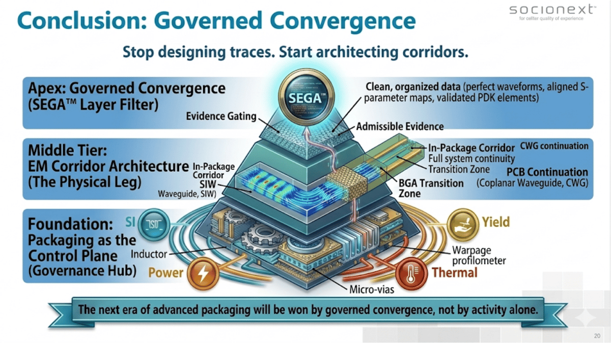
- •Packaging now acts as active control plane for power, thermal, signal integrity
- •Governed convergence needs traceable, deterministic decision architectures across domains
- •Interoperable verification ecosystems lay groundwork for future governance frameworks
Pulse Analysis
The shift from isolated verification flows to a governed convergence model reflects a deeper structural change in semiconductor engineering. As nodes shrink below 5 nm and chiplet ecosystems proliferate, the number of cross‑domain interactions grows non‑linearly, creating an "entropy wall" where traditional project management and design tools falter. This bottleneck is not a lack of compute power but a scarcity of coordinated decision‑making frameworks that can synthesize evidence across SI/PI, thermal, mechanical, and packaging domains.
Artificial intelligence promises to accelerate design cycles, yet when fed fragmented data it can amplify inconsistencies rather than resolve them. Unchecked AI optimizations may produce locally optimal results that destabilize system‑level performance, especially in high‑speed interconnects and advanced packaging where power integrity and signal integrity are tightly coupled. Consequently, the industry is emphasizing evidence‑driven governance—creating queryable, authoritative data layers that bind causality and uncertainty, turning the package from a passive carrier into an active control plane that enforces deterministic outcomes.
Industry leaders are responding with orchestration frameworks such as the SEGA™ (Systematic Engineering Governance Architecture) methodology, which embeds traceability and bounded AI assistance into the design flow. These governance layers aim to preserve deterministic decision pathways across multiple vendors and manufacturing sites, ensuring that chiplet integration, 2.5 D/3 D stacking, and AI accelerator platforms can scale without sacrificing yield or time‑to‑market. As convergence becomes the next scaling frontier, firms that invest in robust governance architectures will secure a decisive edge in the ultra‑competitive semiconductor landscape.
Beyond Tool Interoperability: The Emerging Governed Convergence Problem in Semiconductor Design
Comments
Want to join the conversation?