Inside Nvidia’s Silicon Photonics Roadmap
Key Takeaways
- •NVL1152 will house 1,152 GPUs, 16× NVL72 scale‑up capacity.
- •Nvidia plans to mix copper with silicon photonics for NVLink networking.
- •Feynman GPUs, due 2028, will run on 800‑volt DC rack architecture.
- •$2 billion invested in Lumentum and Coherent to accelerate photonics development.
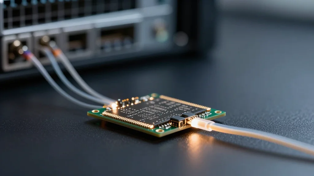
- •Co‑packaged optics will be integrated into NVLink switches for rack‑to‑rack links.
Pulse Analysis
The AI boom is pushing data‑center bandwidth to its limits, exposing copper’s physical constraints beyond roughly two meters. As link speeds climb toward 200 Gb/s, signal loss renders traditional passive copper untenable, prompting industry leaders to explore optical alternatives. Nvidia’s roadmap reflects this shift, leveraging silicon photonics and co‑packaged optics (CPO) to extend NVLink’s reach while preserving the low latency essential for large‑scale model training. By blending copper where feasible and deploying photonic links for longer distances, Nvidia aims to maintain a unified memory space across massive compute clusters.
At the heart of the strategy is the upcoming NVL1152 “Kyber” system, a 1,152‑GPU behemoth that will dwarf the current NVL72 rack. Expected to launch with the 2028 Feynman GPUs, the machine will operate on an 800‑volt DC power architecture, enabling higher compute density while managing the 132‑kW to 220‑kW power envelope of existing racks. The design will likely retain copper interconnects within individual racks but switch to silicon photonics for rack‑to‑rack NVLink connections, using CPO to embed lasers directly onto switch ASICs. This hybrid approach promises a 10× connectivity boost over scale‑out solutions, crucial for training next‑generation AI models that demand unprecedented data throughput.
Nvidia’s aggressive investment—$2 billion split between Lumentum and Coherent—underscores its commitment to building a robust photonics ecosystem. Partnering with TSMC’s COUP platform and a network of over 20 vendors, Nvidia is positioning itself to control both the silicon and optical layers of future AI hardware. As competitors scramble to adopt similar technologies, Nvidia’s early lead could translate into market dominance in high‑performance AI infrastructure, influencing everything from cloud providers to enterprise data centers. The convergence of higher‑voltage power, advanced packaging, and integrated optics marks a pivotal evolution in the compute stack, setting the stage for the next wave of AI breakthroughs.
Inside Nvidia’s Silicon Photonics Roadmap
Comments
Want to join the conversation?