A Closer Look at Huawei’s Chip Design Workaround without EUV
Companies Mentioned
Why It Matters
By circumventing EUV dependence, Huawei can sustain chip advancement under export restrictions, potentially reshaping global semiconductor roadmaps and influencing rivals facing similar supply constraints.
Key Takeaways
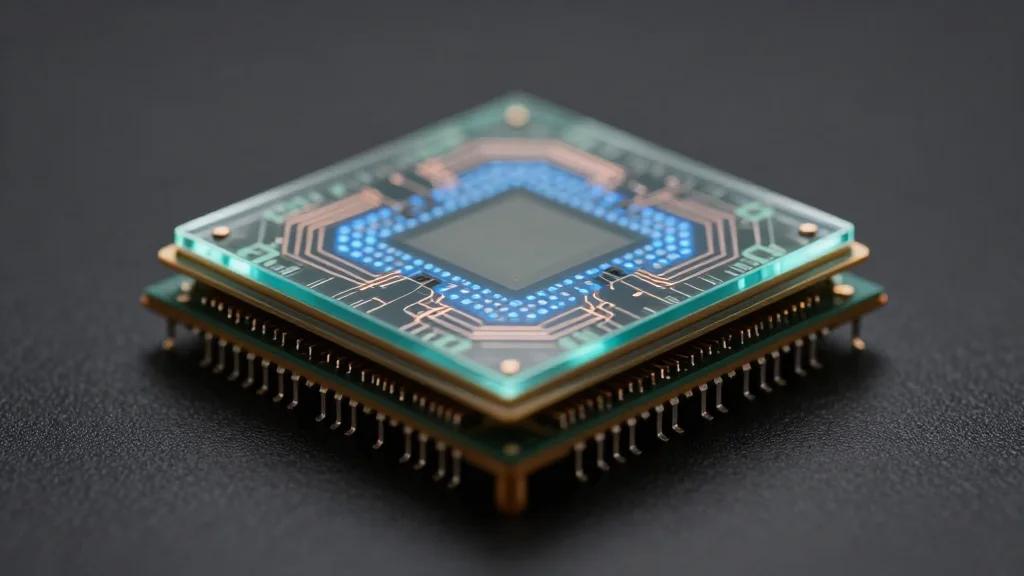
- •Huawei's LogicFolding uses 3D stacking to replace EUV lithography
- •1.4 nm node targeted for 2031 despite current technology limits
- •Hybrid bonding enables dense interconnects without extreme‑ultraviolet tools
- •Strategy could reshape semiconductor roadmaps amid US export restrictions
- •Industry watches for performance gains versus increased manufacturing complexity
Pulse Analysis
The semiconductor industry has long depended on EUV lithography to push transistor dimensions below 5 nm. With the United States tightening export controls on EUV machines, Chinese firms like Huawei face a critical technology gap. Rather than waiting for policy shifts, Huawei is engineering a parallel path that leverages vertical integration—stacking multiple logic layers in a single footprint. This 3D approach, branded LogicFolding, reduces reliance on single‑patterning steps and promises higher transistor density without the costly EUV exposure cycles.
At the heart of LogicFolding is hybrid bonding, a technique that creates atomic‑scale connections between stacked wafers. By aligning copper pads and using low‑temperature annealing, the process achieves inter‑die resistance far lower than traditional TSV (through‑silicon via) methods. The result is a chip that can approach a 1.4 nm equivalent node by effectively multiplying the transistor count per unit area. While the target year of 2031 seems distant, the incremental milestones—such as 2 nm and 1.8 nm prototypes—could arrive sooner, giving Huawei a runway to demonstrate performance gains in AI accelerators and 5G baseband processors.
If successful, Huawei’s workaround could ripple across the broader ecosystem. Competitors constrained by similar export bans may adopt 3D stacking and hybrid bonding to offset EUV shortages, potentially accelerating a shift toward heterogeneous integration as the new scaling norm. However, the approach introduces manufacturing complexity, higher yield risks, and substantial capital investment in advanced packaging fabs. Investors and policymakers will watch closely to see whether Huawei can translate the technical promise into commercial chips that challenge the EUV‑driven incumbents.
A closer look at Huawei’s chip design workaround without EUV
Comments
Want to join the conversation?
Loading comments...