A Conversation with GF’s Pioneer Silicon Photonics Leader and Optica Fellow Dr. Yusheng Bian
Companies Mentioned
Why It Matters
Silicon photonics is becoming the backbone of next‑generation data‑center and emerging‑tech architectures, and GF’s scale and IP leadership position it to set industry standards and capture growing market share.
Key Takeaways
- •GF now the world’s largest pure‑play silicon photonics foundry
- •AI‑driven data centers push silicon photonics beyond copper limits
- •Co‑packaged optics bring optical engines closer to ASICs for higher density
- •GF’s AMF and Infinilink acquisitions expand global capacity and IP portfolio
- •Roadmap targets 400 Gbps per lane, cutting power and latency
Pulse Analysis
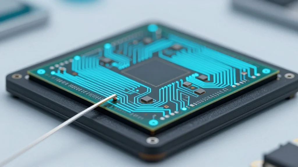
The surge in artificial‑intelligence workloads is straining traditional copper interconnects, prompting data‑center operators to adopt silicon‑photonic solutions that deliver higher bandwidth, lower latency, and dramatically reduced power consumption. GlobalFoundries leverages its 300 mm CMOS platform to integrate optical functions directly on silicon, enabling pluggable optical engines that already generate billions in revenue for giants like Google and NVIDIA. This convergence of electronics and photonics not only solves immediate data‑center bottlenecks but also creates a scalable foundation for future compute architectures.
Beyond the data‑center, GF’s strategic acquisitions of AMF and Infinilink have broadened its geographic footprint and enriched its intellectual‑property portfolio, cementing its status as the largest pure‑play silicon‑photonics foundry by revenue. The expanded capability set supports a diverse ecosystem, from co‑packaged optics that place photonic engines next to ASICs, to custom IP blocks for quantum‑computing platforms and chip‑scale LiDAR sensors for autonomous vehicles. These moves illustrate how a foundry‑centric model can accelerate time‑to‑market for complex, multidisciplinary applications.
Looking ahead, the industry’s technical roadmap targets data‑rates of 400 Gbps per lane while cutting power per bit, a leap that demands advances in device physics, packaging, and manufacturing yield. GlobalFoundries’ deep expertise in high‑volume CMOS production positions it to meet these challenges, offering customers a reliable path from prototype to mass production. As silicon photonics matures, its role will expand from a niche interconnect technology to a core component of quantum, sensing, and AI‑driven systems, reshaping the semiconductor landscape for the next decade.
A conversation with GF’s pioneer silicon photonics leader and Optica Fellow Dr. Yusheng Bian
Comments
Want to join the conversation?
Loading comments...