A New Approach for 10 kV GaN
Why It Matters
The simplified, low‑cost process makes high‑voltage GaN devices commercially viable, offering higher efficiency and smaller footprints than silicon or SiC alternatives. This could accelerate adoption of GaN in grid‑scale converters, wind‑turbine drives, and high‑voltage power supplies.
Key Takeaways
- •Plasma‑based edge termination eliminates etching for 10 kV GaN devices
- •Breakdown voltage reaches 9.5 kV, 3 kV higher than baseline
- •On‑resistance scales linearly with anode‑to‑cathode length
- •Capacitance 4.2 pF mm⁻¹ enables up to 8.4 GHz cut‑off
- •Compatible with low‑cost substrates like sapphire and silicon
Pulse Analysis
GaN has reshaped low‑voltage power electronics, but scaling its performance to the 10 kV class has remained elusive. Traditional silicon IGBTs and SiC MOSFETs can handle high voltages, yet they suffer from high switching losses, costly substrates, and thick epitaxial layers. The industry seeks a material that combines high breakdown voltage, fast switching, and a compact form factor—attributes that GaN’s wide bandgap and two‑dimensional electron gas naturally provide. However, existing high‑voltage GaN designs rely on complex vertical structures or intricate edge‑termination schemes that drive up manufacturing expense and reduce yield.
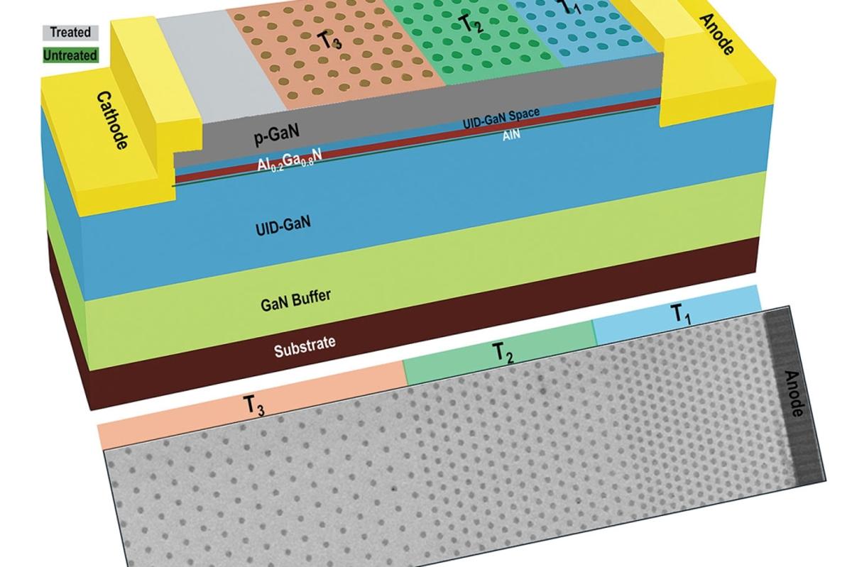
The Ariona State University team tackles this bottleneck with a plasma‑based edge termination that sidesteps etching and additional passivation. By selectively hydrogen‑charging the top p‑GaN layer, they create resistive zones that smooth the electric field at device edges, dramatically reducing peak stress. Simulations and fabricated prototypes confirm a jump from 5.3 kV to 9.5 kV breakdown voltage, while maintaining a modest 1.1 V turn‑on voltage and an on/off ratio of 10¹⁰. The devices also exhibit low on‑resistance that scales predictably with anode‑to‑cathode length, and a capacitance of 4.2 pF mm⁻¹ that supports gigahertz‑range switching frequencies.
If the approach scales to volume production, it could lower the cost barrier for high‑voltage GaN power modules, enabling lighter, more efficient converters for electric grids, renewable‑energy inverters, and industrial drives. The compatibility with inexpensive substrates such as sapphire or silicon further widens its market appeal, potentially displacing silicon IGBTs and SiC devices in applications where size, efficiency, and thermal management are critical. Future work on dynamic switching, long‑term reliability, and packaging will determine how quickly this technology moves from the lab to commercial power‑electronics portfolios.
A new approach for 10 kV GaN
Comments
Want to join the conversation?
Loading comments...