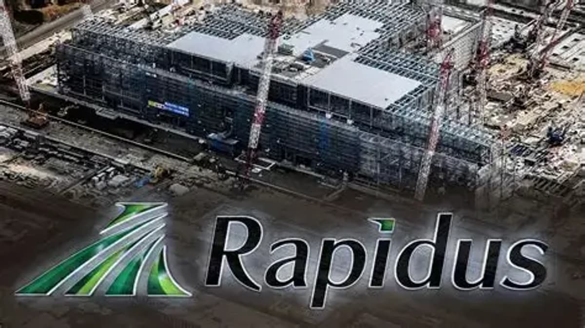
Accelerating 2nm & Advanced Packaging Through Global Collaboration


Why It Matters
Rapidus’ AI‑enabled, end‑to‑end manufacturing platform could become a strategic differentiator for AI and HPC chip makers, compressing time‑to‑market and reducing reliance on a handful of legacy fabs. Its global partnership approach also bolsters supply‑chain resilience amid geopolitical tensions.
Key Takeaways
- •Rapidus aims to cut design qualification from a year to months
- •AI-driven fab predicts yield deviations and optimizes equipment in real time
- •Integrated 2nm wafer and 3D packaging reduces time‑to‑market for AI chips
- •Global partnership network strengthens supply‑chain resilience and sustainability
Pulse Analysis
The surge in artificial‑intelligence workloads is driving semiconductor revenue toward $1.3 trillion this year, according to Gartner, and forcing the industry to confront the limits of traditional, high‑volume fabs. As AI models become larger and more power‑hungry, chipmakers need nodes that deliver unprecedented performance per watt. The 2nm process, paired with heterogeneous integration, offers that efficiency, but its development costs and technical complexity exceed the capacity of any single foundry. Consequently, a collaborative, data‑centric manufacturing model is emerging as a practical solution to meet escalating demand.
Rapidus is betting on an "AI Foundry" that turns the fab into a living system. By outfitting equipment with thousands of sensors and feeding real‑time data into predictive algorithms, the company can anticipate yield drift, dynamically tune process parameters, and co‑optimize design and manufacturing steps. This reduces the typical twelve‑to‑eighteen‑month qualification timeline to a matter of weeks, giving startups and research labs the agility historically reserved for internal chip design teams. The integrated wafer‑to‑package flow further eliminates hand‑off delays, allowing 2nm logic to be stacked with memory, RF and photonic components in a single 3D package.
Beyond speed, Rapidus’ model addresses two strategic pressures: supply‑chain security and sustainability. By forging partnerships across Asia, Europe and the United States, the firm diversifies critical inputs—from lithography tools to advanced materials—mitigating geopolitical risk. Its commitment to renewable energy, water‑reduction technologies and low‑power device architectures also positions the company to meet tightening ESG expectations. If successful, this collaborative, AI‑driven approach could redefine the foundry business, making advanced nodes more accessible and fostering a more resilient, environmentally conscious semiconductor ecosystem.
Accelerating 2nm & Advanced Packaging through global collaboration
Comments
Want to join the conversation?
Loading comments...