ACM Research Ships First PECVD SiCN System for Advanced Semiconductor Applications
Companies Mentioned
Why It Matters
The debut of a three‑station PECVD tool gives chipmakers tighter process control for sub‑55 nm nodes, accelerating adoption of SiCN films in high‑performance BEOL and advanced packaging, a fast‑growing market segment.
Key Takeaways
- •World's first three‑station PECVD design improves film uniformity
- •One Station, One RF software enables independent plasma control
- •Supports 300‑mm wafers, up to 400 °C for advanced BEOL
- •Targets copper diffusion barriers, etch‑stop and wafer‑level bonding
- •Positions ACM for growth in advanced packaging applications
Pulse Analysis
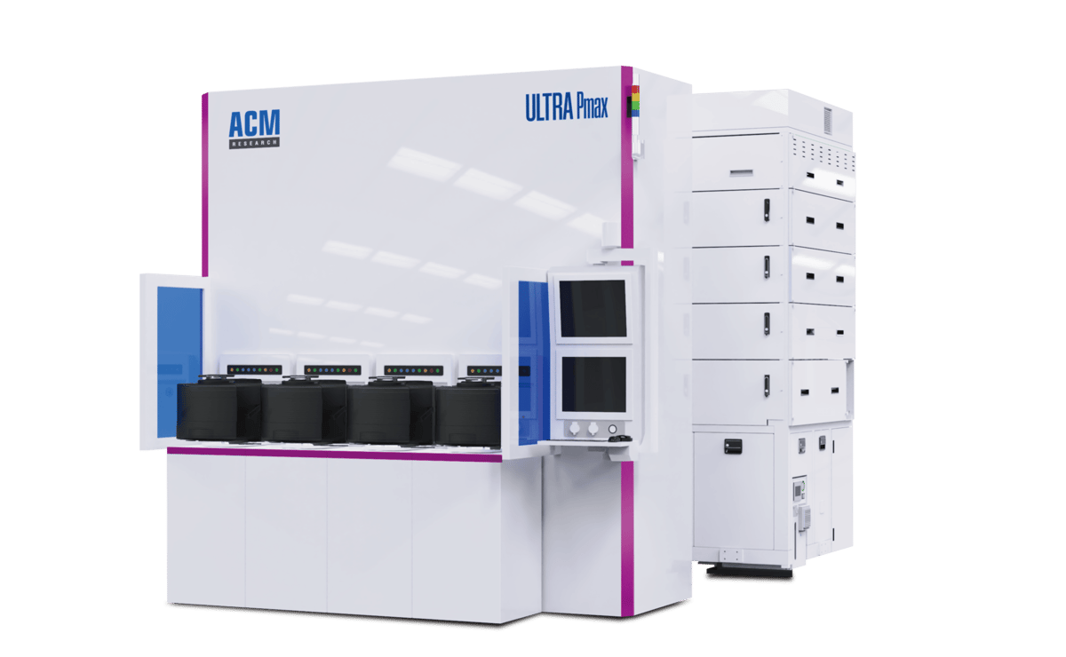
The semiconductor industry is racing toward sub‑55 nm logic and heterogeneous integration, driving demand for materials that can withstand tighter design rules and higher device density. Silicon carbonitride (SiCN) has emerged as a preferred dielectric and barrier material because of its high adhesion, low ion diffusion, and robust mechanical properties. ACM Research’s new PECVD SiCN system arrives at a moment when manufacturers are seeking equipment that can deliver consistent film quality across large 300‑mm wafers while maintaining process flexibility for diverse BEOL steps.
ACM’s breakthrough lies in its three‑station deposition architecture, a departure from traditional single‑zone PECVD reactors. By allocating one‑third of the film growth to each of three rotating stations, the system achieves finer control over gas flow dynamics, plasma stability, and interface formation. The accompanying “One Station, One RF” software provides dedicated radio‑frequency power to each zone, reducing cross‑talk and enhancing repeatability. These innovations translate into tighter thickness tolerances, lower particle contamination, and improved yield—critical factors for copper diffusion barriers and etch‑stop layers in advanced nodes.
Beyond BEOL, the SiCN platform is poised to support wafer‑level bonding in next‑generation packaging, where dense, high‑energy films are essential for reliable interconnects and thermal management. As chipmakers expand into 2.5‑D and 3‑D integration, the ability to deposit uniform SiCN layers quickly becomes a competitive advantage. ACM’s entry into this niche not only broadens its product portfolio but also signals a strategic push into the high‑growth advanced packaging market, where equipment suppliers can capture significant revenue as the industry scales beyond traditional planar architectures.
ACM Research Ships First PECVD SiCN System for Advanced Semiconductor Applications
Comments
Want to join the conversation?
Loading comments...