Advantest Opens Strategic Innovation Centre
Companies Mentioned
Why It Matters
The center speeds creation of reliable test solutions for increasingly complex AI and HPC chips, helping semiconductor firms shorten time‑to‑market and improve yield in a competitive landscape.
Key Takeaways
- •San Jose Innovation Center now operational, Sunnyvale opening summer
- •Facilities include clean rooms, advanced test insertions for complex packaging
- •Enables early‑stage collaboration across semiconductor supply chain
- •Targets AI, HPC, edge markets with faster, reliable test solutions
Pulse Analysis
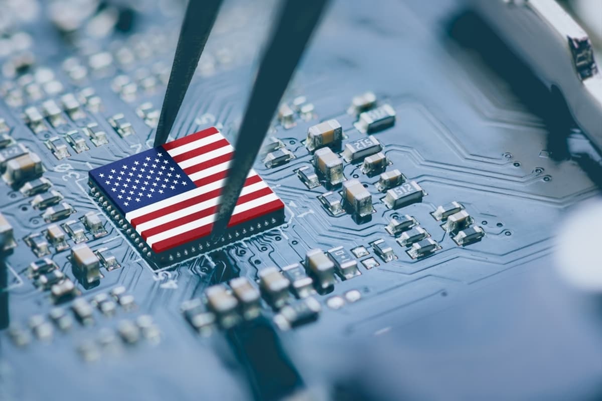
Advantest, a leading provider of semiconductor test equipment, announced the opening of its first Innovation Center in San Jose, with a second site slated for Sunnyvale later this summer. The move comes as AI‑driven workloads, high‑performance computing, and edge devices push chip architectures toward ever‑greater transistor density and advanced packaging techniques such as 2.5‑D and 3‑D integration. Traditional test methodologies struggle to keep pace, creating a market gap for more flexible, high‑throughput validation platforms. By situating cutting‑edge labs at the heart of Silicon Valley, Advantest positions itself to address this gap and capture growing demand for next‑generation test solutions.
The Innovation Center offers clean‑room environments, state‑of‑the‑art test insertions, and a suite of measurement tools designed for complex device architectures. What sets the facility apart is its collaborative model: semiconductor manufacturers, packaging firms, and material suppliers can work side‑by‑side with Advantest engineers from early design stages through pilot production. This hands‑on partnership reduces iteration cycles, aligns roadmaps, and accelerates the qualification of new test methodologies. Early adopters have already signed agreements, signaling strong industry appetite for a shared R&D hub that blends equipment expertise with supply‑chain insights.
For the broader ecosystem, the centers promise faster time‑to‑market for AI and HPC chips, translating into competitive advantage for customers that rely on rapid innovation cycles. Advantest’s approach also mirrors a wider trend toward co‑development labs, as seen with rivals like Teradyne and ASML, which are investing in similar collaborative spaces. If the Sunnyvale site launches as planned, the dual‑location network could become a de‑facto standard for semiconductor test development, driving industry‑wide improvements in reliability, yield, and cost efficiency. Analysts expect Advantest’s revenue to benefit from increased service contracts and longer‑term equipment leases tied to these collaborative projects.
Advantest opens Strategic Innovation Centre
Comments
Want to join the conversation?
Loading comments...