Aixtron’s CCS R&D System to Be Centerpiece of Penn State’s New Semiconductor Lab
Companies Mentioned
Why It Matters
The collaboration strengthens the U.S. semiconductor supply chain by expanding domestic R&D capacity and aligns with the CHIPS Act’s goal of fostering advanced manufacturing and a skilled workforce. It also gives industry and academia a shared platform to accelerate commercialization of GaN‑based power devices and 2D‑material AI hardware.
Key Takeaways
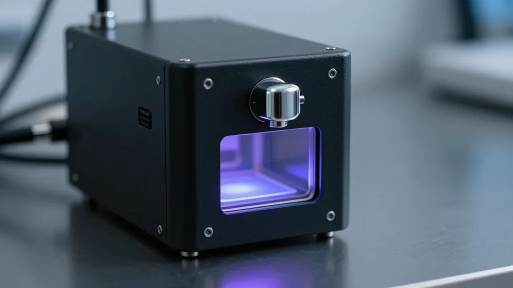
- •Aixtron’s CCS system installed at Penn State’s Materials Research Institute
- •$4.3 million federal and in‑kind funding supports the new lab
- •System deposits GaN and 2D materials on 100 mm wafers
- •Enables research from material fundamentals to prototype devices
- •Provides national user platform and workforce training for researchers
Pulse Analysis
The partnership between Aixtron and Penn State arrives at a pivotal moment for U.S. microelectronics policy. Backed by $4.3 million in federal infrastructure funds and the Midwest Microelectronics Consortium, the new lab fulfills a core objective of the CHIPS Act: to rebuild domestic semiconductor research capacity and reduce reliance on overseas fabs. By situating the facility within the university’s Millennium Science Complex, the initiative creates a hub that can attract both academic investigators and defense‑related projects under the DoD‑sponsored Microelectronics Commons program.
Technically, the Close Coupled Showerhead (CCS) system offers a rare combination of wide‑bandgap gallium nitride (GaN) and two‑dimensional (2D) material deposition on 100 mm substrates. This dual capability shortens the development cycle for power‑electronics components used in electric vehicles and renewable‑energy converters, while also enabling experimental platforms for AI accelerators and neuromorphic chips that rely on atomically thin semiconductors. The high‑precision epitaxial growth environment ensures layer uniformity and defect control, critical factors for scaling next‑generation devices from lab prototypes to commercial products.
Beyond the hardware, the lab is positioned as a national user platform that will train the next generation of semiconductor engineers. Hands‑on access to industry‑grade equipment, combined with mentorship from Penn State’s 2D Crystal Consortium, addresses the talent gap highlighted by industry leaders. By fostering collaboration between academia, government, and private firms, the facility not only accelerates innovation but also reinforces the U.S. supply chain, ensuring that breakthroughs in GaN power devices and 2D‑material computing can be rapidly transitioned to market.
Aixtron’s CCS R&D system to be centerpiece of Penn State’s new semiconductor lab
Comments
Want to join the conversation?
Loading comments...