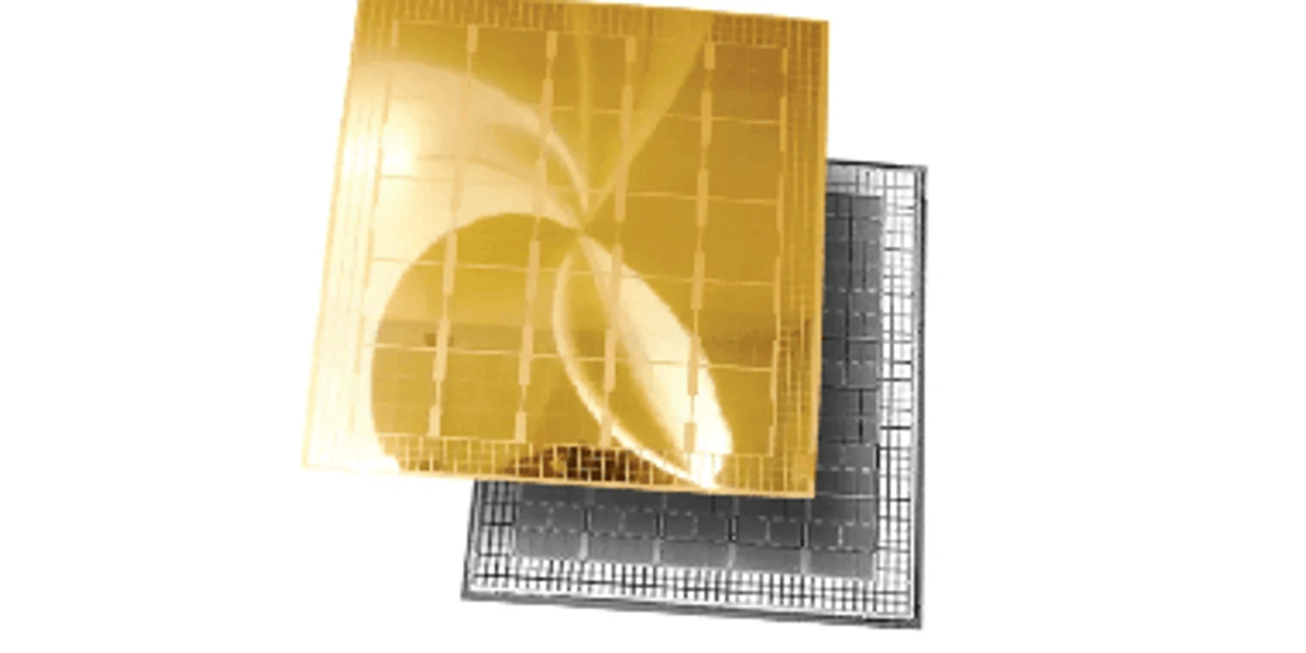
ASE Launches Automated 310mm Panel-Level Packaging to Accelerate AI Innovation
Why It Matters
The panel‑level approach unlocks greater integration density and throughput, accelerating AI and HPC product rollouts while lowering manufacturing costs. This gives ASE a competitive edge as chiplet‑based designs become the industry standard.
Key Takeaways
- •ASE unveils first automated 310mm panel packaging line, production H1 2027.
- •Panel format adds 96,100 mm² area, boosting die count per run.
- •Supports FOCoS and FOCoS‑Bridge with 2 µm line/space precision.
- •Enhances AI/HPC throughput, reducing cycle time and material waste.
- •Positions ASE ahead in heterogeneous chiplet integration market.
Pulse Analysis
Panel‑level packaging is emerging as the next logical step after wafer‑level processes, offering a larger substrate that can host more dies and interconnects. ASE’s 310 mm × 310 mm line delivers 96,100 mm² of usable area, roughly 30% more than a standard 200 mm wafer, and maintains tight line‑space tolerances (2 µm for FOCoS, 8 µm for FOCoS‑Bridge). This scale‑up reduces per‑die material waste, cuts tool‑change steps, and shortens overall cycle time, addressing the efficiency bottlenecks that have constrained AI and high‑performance computing (HPC) manufacturers.
For AI accelerators and HPC chips, the ability to integrate more chiplets, ASICs, and high‑bandwidth memory (HBM) on a single package is critical to achieving the bandwidth and latency targets of next‑generation workloads. ASE’s panel platform enables higher I/O density and supports heterogeneous integration, allowing designers to build trillion‑transistor system‑in‑package (SiP) architectures without sacrificing yield. The larger panel also facilitates the use of larger interposers, a key requirement as AI models grow in complexity and data‑center customers demand ever‑greater compute density.
ASE’s early move into automated panel‑level production positions it ahead of rivals still focused on wafer‑centric solutions. By aligning its roadmap with industry standards for chiplet‑based designs, ASE can offer faster time‑to‑market and lower total cost of ownership for hyperscale customers. As the ecosystem matures, we can expect broader adoption of panel‑level packaging across networking, gaming and edge AI segments, further cementing ASE’s role as a critical enabler of the AI‑driven semiconductor renaissance.
ASE Launches Automated 310mm Panel-Level Packaging to Accelerate AI Innovation
Comments
Want to join the conversation?
Loading comments...