Asymmetry Spawns Superior SiC Superjunctions
Why It Matters
Accurate anisotropy‑aware modeling unlocks higher efficiency in SiC power devices, directly improving the performance and cost profile of renewable‑energy inverters and EV drivetrains. Faster design cycles reduce R&D spend and accelerate market adoption of next‑gen power electronics.
Key Takeaways
- •Asymmetric SiC superjunctions cut specific on‑resistance up to 19% versus symmetric designs
- •Impact‑ionisation anisotropy must be modeled; isotropic assumptions overestimate breakdown voltage
- •Unified analytical framework solves Poisson’s equation, slashing simulation time from hours to seconds
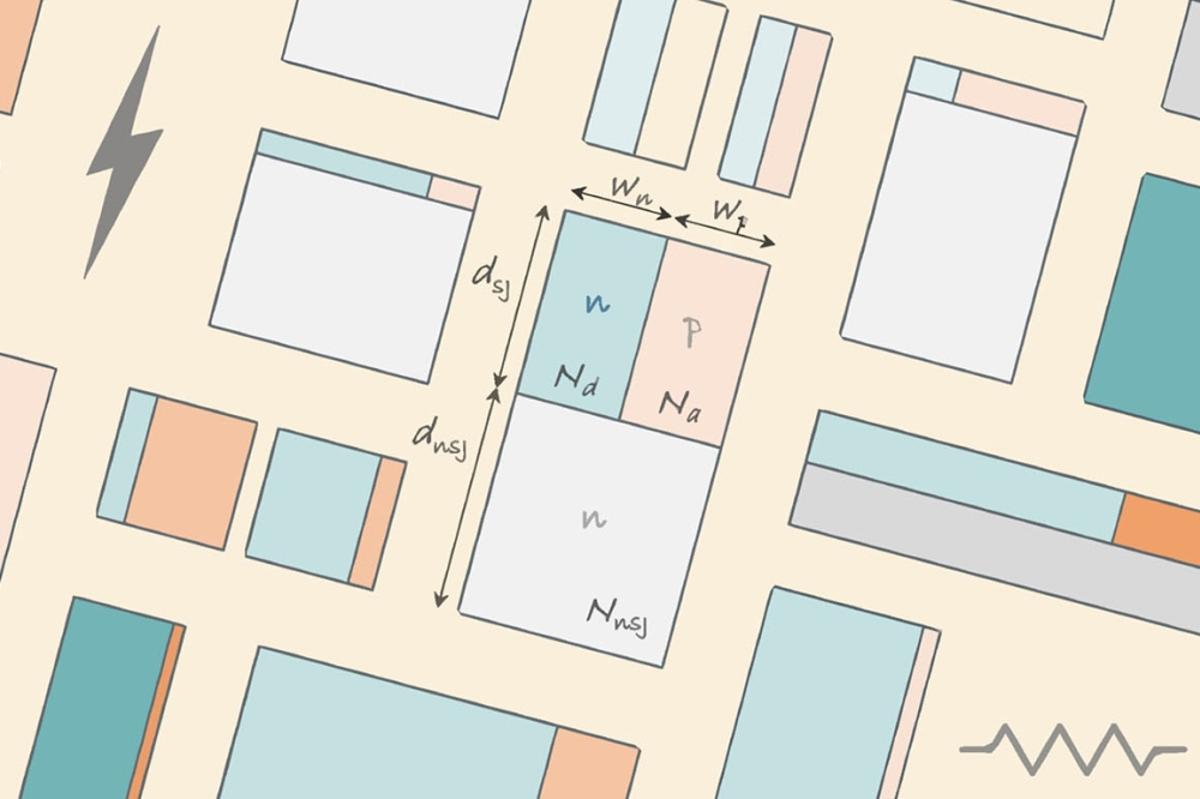
- •Wider n‑pillars with higher p‑doping preserve voltage while lowering resistance
- •Semi‑superjunctions become more practical, offering cost‑effective manufacturing
Pulse Analysis
The surge in global electricity demand, driven by electric‑vehicle adoption and data‑center expansion, places unprecedented pressure on power‑conversion efficiency. Silicon‑carbide (SiC) devices already enjoy a material advantage—wide bandgap, high critical electric field, and superior thermal conductivity—making them ideal for high‑voltage, high‑temperature applications. Yet, conventional SiC superjunction designs have been hamstrung by the classic trade‑off between specific on‑resistance and breakdown voltage, and by design tools that ignore the pronounced anisotropy of impact ionisation in SiC crystals. By explicitly accounting for the directional differences in electron and hole avalanche coefficients, Rohm’s new model delivers realistic blocking‑voltage predictions, closing a critical gap between theory and real‑world device behavior.
Beyond physics fidelity, the real innovation lies in the framework’s analytical treatment of geometric asymmetry. Traditional symmetric designs simplify charge balance but rarely reflect manufacturing realities, where pillar widths and dopant concentrations vary. Rohm’s approach derives exact solutions to Poisson’s equation, producing closed‑form expressions for electric‑field distribution and specific on‑resistance. This enables engineers to explore a vast design space—adjusting n‑pillar width, p‑pillar doping, and drift‑region dimensions—in seconds on a standard CPU, a stark contrast to the hours required for conventional TCAD runs. The result is a systematic pathway to asymmetric semi‑superjunctions that achieve up to a 19% reduction in on‑resistance while maintaining comparable breakdown voltages.
The commercial implications are substantial. Lower on‑resistance translates directly into higher system‑level efficiency for renewable‑energy converters and EV inverters, reducing losses and heat dissipation. Faster, cost‑effective design cycles shorten time‑to‑market and lower R&D expenditures, making SiC solutions more competitive against silicon alternatives. As manufacturers embed this anisotropy‑aware, asymmetry‑tuned methodology into their development pipelines, the industry can expect accelerated adoption of higher‑voltage SiC platforms, supporting the broader transition to cleaner, more efficient power infrastructure.
Asymmetry spawns superior SiC superjunctions
Comments
Want to join the conversation?
Loading comments...