Carbon Nanotube Coating Creates On-Chip Terahertz Waveguides
Companies Mentioned
Why It Matters
The breakthrough provides a footprint‑efficient way to manage terahertz signals on silicon, accelerating the integration of high‑frequency components needed for next‑generation wireless standards and high‑speed sensing applications.
Key Takeaways
- •SWCNT coating provides up to 47 dB attenuation at 140‑220 GHz
- •Film thickness 2‑53 nm yields >20 dB reflection loss
- •Record specific shielding efficiency of 5.5 × 10⁹ dB·cm²/g
- •Enables compact, broadband terminations without bulky tapers
- •Supports high‑density on‑chip terahertz circuits for future 6G
Pulse Analysis
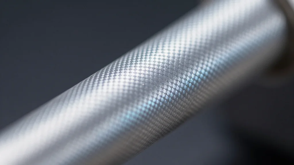
Terahertz frequencies—spanning roughly 100 GHz to 10 THz—bridge the gap between conventional radio and optical domains, promising ultra‑wide bandwidth for communications, imaging, and spectroscopy. Yet the wavelengths are too short for traditional electronic interconnects and too long for purely photonic components, forcing engineers to rely on waveguides that can confine and guide the energy. Conventional on‑chip terminations use adiabatic tapers that gradually expand the mode into free space, a method that consumes valuable silicon real estate and can radiate unwanted energy, limiting integration density.
The Skolkovo‑KTH team tackled this bottleneck by depositing an ultrathin single‑walled carbon nanotube film onto silicon dielectric rod waveguides. Produced via a floating‑catalyst aerosol CVD process, the SWCNT layers as thin as 2 nm and as thick as 53 nm act as a near‑perfect absorber, delivering up to 47 dB of attenuation while keeping reflections below 20 dB across the 140‑220 GHz band. This performance translates to a specific shielding efficiency of 5.5 × 10⁹ dB·cm²/g, a record that underscores the material’s ability to suppress electromagnetic leakage without the bulk of traditional tapers. The result is a compact, broadband termination that preserves chip area and reduces electromagnetic pollution, a critical advantage for densely packed terahertz circuits.
Beyond the laboratory, the technology aligns with the roadmap for 6G wireless systems, which anticipate operation deep into the terahertz spectrum to achieve multi‑gigabit per second links and ultra‑low latency. By offering a scalable, silicon‑compatible solution, SWCNT‑based absorbers could accelerate the commercialization of on‑chip terahertz transceivers, sensors, and imaging modules. Industry players eyeing high‑frequency components stand to benefit from reduced packaging complexity and enhanced performance, while further research may explore integration with CMOS processes and the extension of the coating to other terahertz‑compatible substrates.
Carbon nanotube coating creates on-chip terahertz waveguides
Comments
Want to join the conversation?
Loading comments...