CEA-Leti and NcodiN Partner to Industrialise 300 Mm Silicon Photonics
Companies Mentioned

Why It Matters
These initiatives bring wafer‑scale photonic interconnects and advanced non‑volatile memory closer to volume production, addressing the bandwidth‑power bottleneck of AI hardware and reinforcing Europe’s semiconductor sovereignty.
Key Takeaways
- •NcodiN’s nanolaser is 500× smaller than current silicon lasers
- •300 mm photonic interposer aims for ~0.1 pJ/bit energy consumption
- •Fraunhofer‑CEA wafer exchange validates ferroelectric HZO memory on 300 mm CMOS
- •CEA‑List and PSMC will combine RISC‑V IP with silicon‑photonic chiplets
- •FAMES 2026 call adds RF BAW filters and 10 nm FD‑SOI PDKs
Pulse Analysis
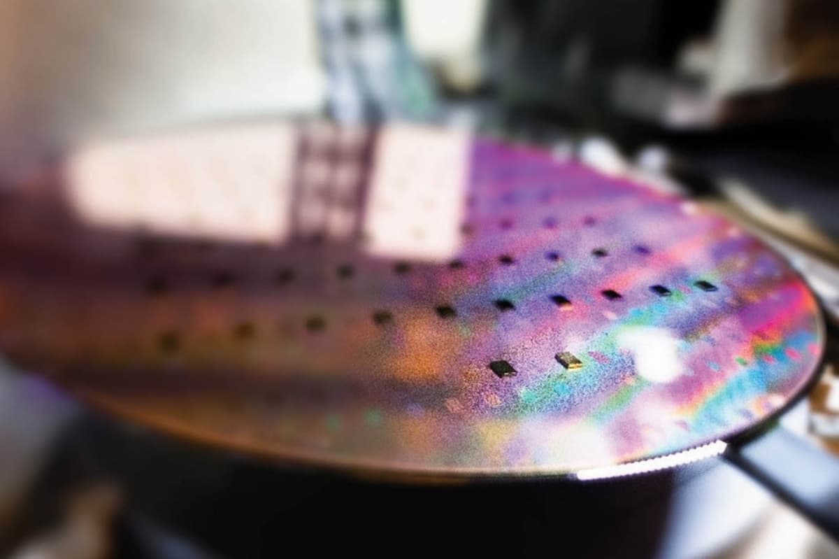
The race to replace copper with light‑based links is accelerating as AI models demand ever‑higher bandwidth and lower energy per bit. NcodiN’s nanolaser, touted as the world’s smallest silicon laser—500 times smaller than conventional devices—promises ultra‑dense integration of more than 5,000 emitters per square millimetre. By moving this technology onto a 300 mm silicon‑photonic wafer, CEA‑Leti aims to achieve sub‑0.1 pJ/bit energy consumption, a metric that could dramatically reduce the power envelope of future AI accelerators while keeping costs compatible with high‑volume manufacturing.
Parallel to the photonics push, European researchers are de‑risking emerging non‑volatile memories through a collaborative wafer‑exchange program between CEA‑Leti and Fraunhofer IPMS. The pilot validated hafnium‑zirconium‑oxide (HZO) ferroelectric capacitors on a 300 mm CMOS platform, demonstrating reliable switching over 10⁷ cycles and paving the way for integration into 22 nm FDX® memory demonstrators. Such ferroelectric‑based FeRAM offers near‑instantaneous write speeds and virtually zero standby power, making it a strong candidate for compute‑in‑memory architectures that aim to keep data close to the processor.
Beyond individual technologies, the broader European ecosystem is consolidating its capabilities. CEA‑List’s RISC‑V expertise, combined with CEA‑Leti’s silicon‑photonic know‑how, will be offered to PSMC for 3D‑stacked AI chips, delivering customizable compute cores alongside high‑bandwidth optical chiplet communication. Meanwhile, the FAMES pilot line’s 2026 Open‑Access Call introduces new RF BAW filter and phase‑change‑material switch PDKs, plus a 10 nm FD‑SOI node, giving innovators a sovereign toolbox to prototype next‑generation radios, power‑management ICs, and low‑power logic. Together, these efforts aim to close the gap between research breakthroughs and commercial silicon, strengthening Europe’s position in the global semiconductor supply chain.
CEA-Leti and NcodiN partner to industrialise 300 mm Silicon Photonics
Comments
Want to join the conversation?
Loading comments...