CEA-Leti to Present Advances in Next-Gen Chip Integration at ECTC 2026
Companies Mentioned

STMicroelectronics Inc.
Why It Matters
Hybrid bonding promises higher density, lower power and new form‑factors, enabling heterogeneous stacks that traditional CMOS cannot achieve. This accelerates the adoption of quantum, 5G/6G and automotive radar technologies that rely on advanced packaging.
Key Takeaways
- •CEA‑Leti demonstrated 1 µm pitch die‑to‑wafer hybrid bonding.
- •Low‑temperature annealing achieved at 100 °C enables heterogeneous integration.
- •Hybrid bonding targets high‑density 3D integration beyond micro‑bump limits.
- •Applications include quantum computing interconnects and millimeter‑wave radar packaging.
- •Papers at ECTC 2026 highlight industry shift toward advanced packaging.
Pulse Analysis
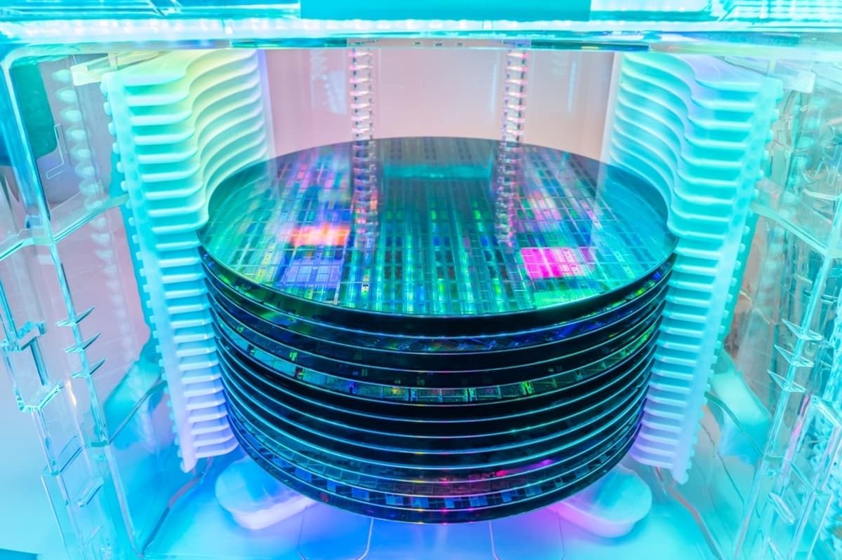
Hybrid bonding has emerged as the linchpin of next‑generation semiconductor integration, offering a path to sub‑micron vertical interconnects that traditional micro‑bump techniques cannot sustain. By directly bonding copper and dielectric layers, manufacturers can achieve pitches as tight as 1 µm, dramatically increasing I/O density while reducing parasitic resistance and capacitance. This technology aligns with the broader industry trend of moving performance gains from transistor scaling to system‑level packaging, a shift driven by the physical limits of Moore's Law.
At the European Conference on Technology and Components (ECTC) 2026, CEA‑Leti will present a suite of innovations that push hybrid bonding into new territory. Their die‑to‑wafer test vehicle demonstrates a 1 µm pitch, while a separate study proves that reliable bonds can be formed at an unprecedented 100 °C annealing temperature. Such low‑temperature processing is critical for integrating temperature‑sensitive materials—polymers, certain III‑V semiconductors, and even superconducting films—into heterogeneous stacks without damaging underlying CMOS circuitry. The ability to fuse disparate technologies on a single platform opens avenues for compact, high‑performance modules across multiple sectors.
The implications extend far beyond academic interest. In quantum computing, superconducting 3D interconnects with minimal thermal resistance are essential for maintaining qubit coherence, and CEA‑Leti’s work directly addresses this need. Meanwhile, fan‑out wafer‑level packaging with integrated antennas supports the millimeter‑wave frequencies required for 5G, emerging 6G, and automotive radar systems. As OEMs and fabless firms race to differentiate their products, the adoption of hybrid bonding is poised to become a competitive advantage, reshaping supply chains and driving new standards in high‑density, low‑power, and multifunctional chip modules.
CEA-Leti to present advances in next-gen chip integration at ECTC 2026
Comments
Want to join the conversation?
Loading comments...