Covalent Expands Wafer-Level Characterization Through Oxford Instruments Collaboration
Companies Mentioned
Why It Matters
By delivering high‑resolution, full‑wafer Raman/PL data in a production‑ready workflow, the collaboration shortens time‑to‑market for next‑generation power devices and reduces costly silicon‑chip failures. It also narrows the gap between R&D labs and high‑volume manufacturing, a critical advantage as compound semiconductors scale.
Key Takeaways
- •Covalent adds wafer‑level Raman/PL to its portfolio via Oxford partnership.
- •Supports 300 mm wafers, enabling full‑wafer defect, stress, strain mapping.
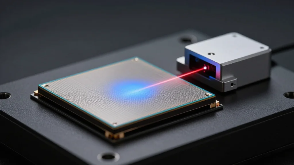
- •Dual‑laser (355 nm & 532 nm) system offers complementary surface‑sensitive analysis.
- •Accelerates yield improvement and failure analysis for SiC, GaN production.
Pulse Analysis
The semiconductor industry is rapidly shifting toward wide‑bandgap materials such as silicon carbide and gallium nitride, driven by demand for high‑efficiency power electronics. Traditional metrology tools struggle to keep pace with the larger wafer sizes and the need for non‑destructive, high‑throughput analysis. Covalent’s new offering, built on Oxford Instruments’ WITec360 Raman platform, directly addresses this gap by delivering full‑wafer Raman and photoluminescence data, allowing engineers to visualize material uniformity and defect patterns across 300 mm substrates in a single pass.
Technically, the dual‑laser configuration—355 nm for surface‑sensitive photoluminescence and 532 nm for deeper Raman scattering—provides complementary insight into crystal quality, doping levels, and stress gradients. The integrated workflow automates data acquisition, processing, and visualization, turning raw spectra into actionable maps that can be fed into statistical process control systems. This reduces the manual effort typically required for separate Raman and PL instruments, cuts measurement time, and improves repeatability, which is essential for high‑volume manufacturing environments.
From a business perspective, the collaboration positions Covalent as a one‑stop solution for semiconductor fabs seeking to scale advanced material production without sacrificing yield. Faster root‑cause analysis and real‑time process monitoring translate into lower scrap rates and shorter development cycles, directly impacting the bottom line. As more OEMs adopt SiC and GaN for electric vehicles and renewable‑energy converters, demand for scalable, high‑resolution wafer‑level metrology is expected to surge, giving Covalent and Oxford a competitive edge in a market projected to grow double‑digit annually.
Covalent expands wafer-level characterization through Oxford Instruments collaboration
Comments
Want to join the conversation?
Loading comments...