Creating A Moore’s Law For AI Scaling
Companies Mentioned
Why It Matters
Without coordinated stack‑level innovation, AI’s exponential compute appetite will outstrip power and thermal limits, jeopardizing profitability and planetary sustainability. The shift also creates a competitive differentiator for firms that can deliver efficient, heterogeneous AI hardware.
Key Takeaways
- •AI scaling requires 10× compute efficiency gain in next decade
- •Full‑stack co‑optimization across algorithms, devices, packaging, and fabrics is essential
- •Edge AI chips adopt 2nm, 6nm, 12nm nodes, cutting voltage to 0.4 V
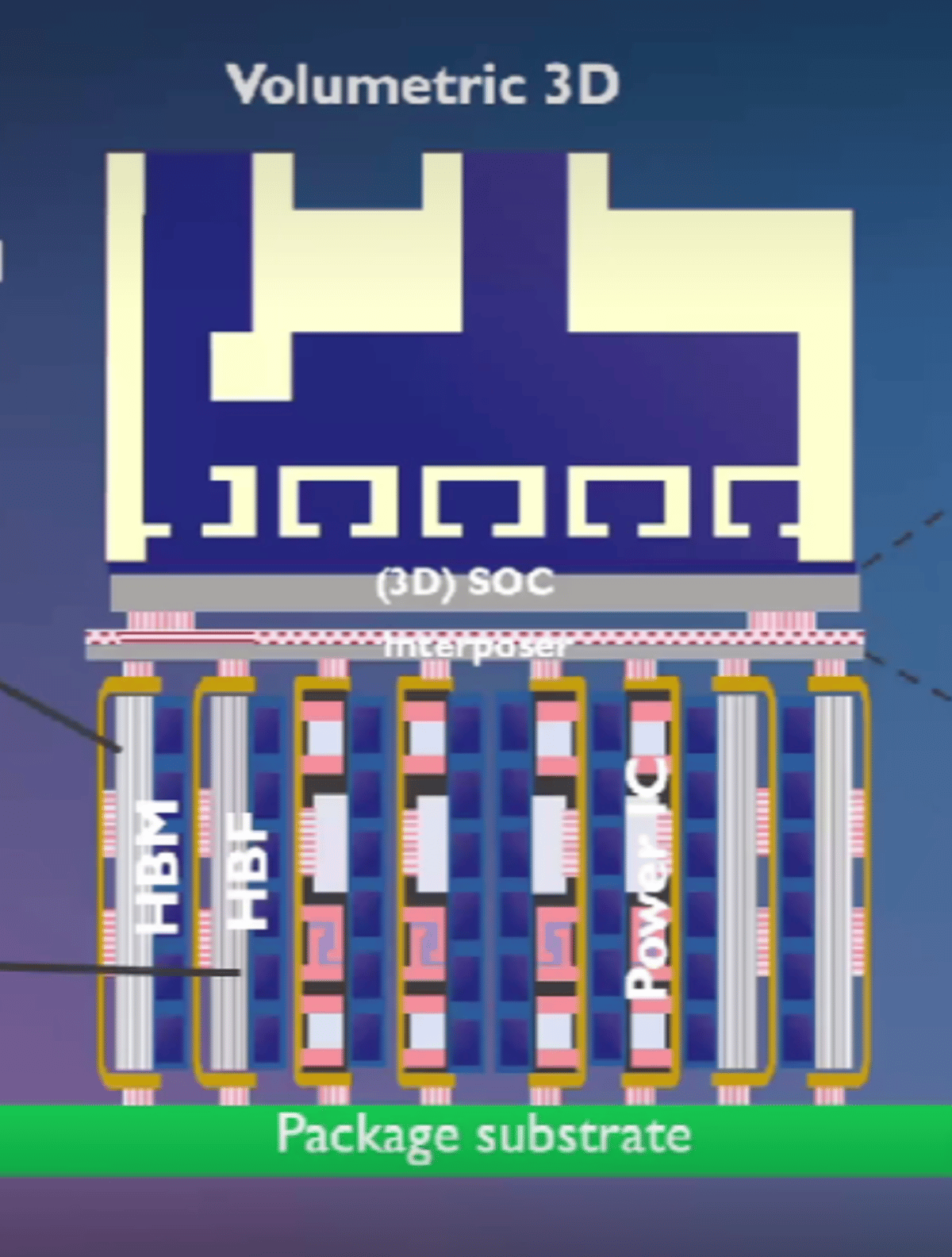
- •Imec roadmap targets 7 Å CFETs and volumetric‑3D interposers by 2033
- •Hybrid bonding and 12‑inch silicon photonics boost bandwidth and yield
Pulse Analysis
The surge in generative and agentic AI models is redefining the compute landscape. Estimates that future multi‑agent systems will require 150 times the processing power of current large language models expose a fundamental scalability bottleneck: traditional data‑center expansion simply adds linear power draw and heat, threatening both cost structures and environmental limits. Industry voices from imec, Samsung and AMD converge on a single premise—only a holistic, full‑stack approach that simultaneously advances algorithms, device physics, packaging and interconnect fabrics can deliver the ten‑fold efficiency gain needed within a decade. This paradigm shift moves the focus from raw transistor count to system‑level optimization.
Key enablers are already emerging on the roadmaps of leading research centers. Imec’s plan to introduce complementary‑FET (CFET) devices at the 7 Å node, combined with active interposers and volumetric‑3D packaging, promises dramatically higher logic density and shorter memory‑to‑compute pathways. Hybrid bonding and 12‑inch silicon‑photonic platforms aim to shrink bandwidth bottlenecks while improving yield and thermal performance. Meanwhile, edge silicon is racing to 2 nm, 6 nm and 12 nm processes, with operating voltages pushed down to 0.4 V to slash switching power by up to 70 %. Together, these advances target the compute‑per‑watt metric that will define AI hardware competitiveness.
The success of this stack‑centric strategy hinges on cross‑industry collaboration. Imec’s open‑innovation model brings together foundries, equipment vendors, EDA firms and device designers to share risk, accelerate validation and align product cycles. Such partnerships reduce time‑to‑market for breakthrough nodes and enable early‑stage co‑design of algorithms and hardware, a necessity for physical AI applications that demand deterministic, microsecond‑scale responses. Companies that embed these co‑optimization practices will not only meet the looming compute demand but also secure a strategic edge as AI hardware becomes the primary differentiator in a market where performance, power and cost are inseparable.
Creating A Moore’s Law For AI Scaling
Comments
Want to join the conversation?
Loading comments...