EC Approves €66m for German SiC Facility
Why It Matters
The funding accelerates critical upstream components—SiC substrates and EUV optics—essential for high‑performance chips, reducing Europe’s reliance on non‑EU suppliers and bolstering its competitive edge in the global semiconductor race.
Key Takeaways
- •Zadient receives $72 million EU grant for SiC source material plant
- •Facility will produce tens of thousands of tons of 8N‑purity SiC annually
- •Circular gas‑recovery process promises higher efficiency and lower carbon footprint
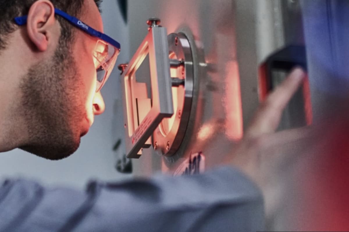
- •Carl Zeiss secures $242 million for EUV lithography optical column scale‑up
- •Funding supports EU's strategic push for autonomous semiconductor supply chain
Pulse Analysis
Europe’s semiconductor strategy has long hinged on closing gaps in the supply chain, and the latest €288 million state‑aid package marks a decisive step toward that goal. By channeling funds into upstream materials and lithography infrastructure, the European Commission is addressing two bottlenecks: the scarcity of ultra‑pure silicon‑carbide (SiC) substrates and the limited domestic capacity for extreme‑ultraviolet (EUV) optical components. Both are indispensable for producing power‑efficient, high‑frequency chips that power everything from electric vehicles to data‑center servers. The aid underscores the EU’s commitment to a self‑sufficient, resilient semiconductor ecosystem that can compete with the United States and Asia.
Zadient Materials Europe’s €66 million grant will establish a Bitterfeld facility capable of manufacturing tens of thousands of tons per year of 8N‑purity SiC source material. The company’s “Sic‑Pro” process recycles process gases, creating a circular system that cuts energy use and lowers emissions—a first of its kind in the EU. By delivering bulk, high‑purity SiC, Zadient aims to enable wafer manufacturers to achieve higher yields and fewer defects, accelerating the rollout of SiC‑based power devices. This aligns with broader market trends where automotive and renewable‑energy sectors demand more efficient power electronics, positioning Europe to capture a growing share of that demand.
The €222 million allocation for Carl Zeiss’s HNA@SCALE project targets the industrialisation of EUV optical columns, a critical component of the lithography machines supplied by Dutch giant ASML. By scaling up production of these precision optics within Europe, the initiative reduces dependence on external suppliers and shortens the lead time for next‑generation chip manufacturing. The move also strengthens the EU’s position in the high‑value EUV ecosystem, fostering innovation clusters around advanced photonics and materials science. Together, the SiC and EUV investments create a synergistic foundation that could transform Europe into a full‑stack semiconductor hub, attracting further private capital and talent to the region.
EC approves €66m for German SiC facility
Comments
Want to join the conversation?
Loading comments...