Fraunhofer IPMS Develops Wafer-Level Chiplet Systems
Why It Matters
QMI promises dramatically higher interconnect density and design flexibility, shortening time‑to‑market for complex electronic systems. It strengthens Europe’s position in the global chiplet ecosystem and could lower production costs for automotive, IoT and consumer‑electronics manufacturers.
Key Takeaways
- •Fraunhofer IPMS demonstrates wafer-level quasi‑monolithic chiplet integration
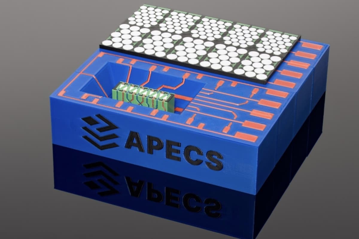
- •Chiplets placed in silicon pockets, then leveled for BEOL wiring
- •Higher interconnect density than traditional packaging, enabling compact systems
- •APECS pilot line funded with €730 million (~$796 million) across Europe
Pulse Analysis
The semiconductor industry is rapidly embracing chiplet architectures as a way to sidestep the escalating costs of monolithic die scaling. By stitching together pre‑validated functional blocks, designers can mix and match technologies, shorten development cycles, and mitigate yield risks. However, integrating disparate chiplets at high density has remained a bottleneck, with conventional packaging limiting interconnect pitch and adding form‑factor overhead. Europe’s response, embodied in the APECS initiative, seeks to close this gap by fostering advanced packaging solutions that rival the agility of Asian foundries.
Fraunhofer IPMS’s quasi‑monolithic integration (QMI) tackles the bottleneck head‑on. The team engineers silicon wafers with precisely etched recesses—"pockets"—into which miniature chiplets are placed. A passivation layer then planarises the surface, allowing subsequent back‑end‑of‑line (BEOL) wiring to be deposited directly on a unified substrate. Because the interconnect stack is formed during the front‑end‑of‑line process, connection densities far exceed those achievable with flip‑chip or interposer methods, delivering a true monolithic feel while preserving the modularity of chiplet design.
The broader market implications are significant. With APECS backed by roughly $796 million in EU funding, the QMI workflow can be scaled from prototype to high‑volume production, attracting automotive, industrial IoT and consumer‑electronics players that demand compact, high‑performance modules. Early adopters stand to benefit from reduced bill‑of‑materials, faster time‑to‑market, and a more resilient supply chain that leverages European wafer‑fab capacity. As the chiplet paradigm matures, technologies like QMI will likely become the standard bridge between heterogeneous components and the next generation of ultra‑dense electronic systems.
Fraunhofer IPMS develops wafer-level chiplet systems
Comments
Want to join the conversation?
Loading comments...