High-Throughput Diffuse Electron Projection Lithography
Why It Matters
DEPL could dissolve the long‑standing resolution‑throughput trade‑off in electron‑beam lithography, enabling sub‑5 nm chip production at wafer‑scale speeds while cutting capital expenses for fabs.
Key Takeaways
- •DEPL achieves 4 nm resolution without electron optics
- •Throughput reaches 15 4‑inch wafers/hour now
- •Scalable to 532 12‑inch wafers/hour potential
- •Uses air‑based beam, cutting vacuum and equipment costs
Pulse Analysis
The semiconductor industry has relied on extreme ultraviolet lithography (EUVL) to push device dimensions below 10 nm, yet EUVL faces escalating cost and complexity as feature sizes approach the physical limits of photon‑based exposure. Electron‑beam lithography offers sub‑2 nm resolution, but its adoption has been hampered by inherently low throughput, a consequence of the narrow, focused beams and the need for high‑vacuum, electron‑optics columns. This bottleneck has left a gap for a post‑EUV solution that can deliver both nanometer precision and manufacturing‑scale productivity.
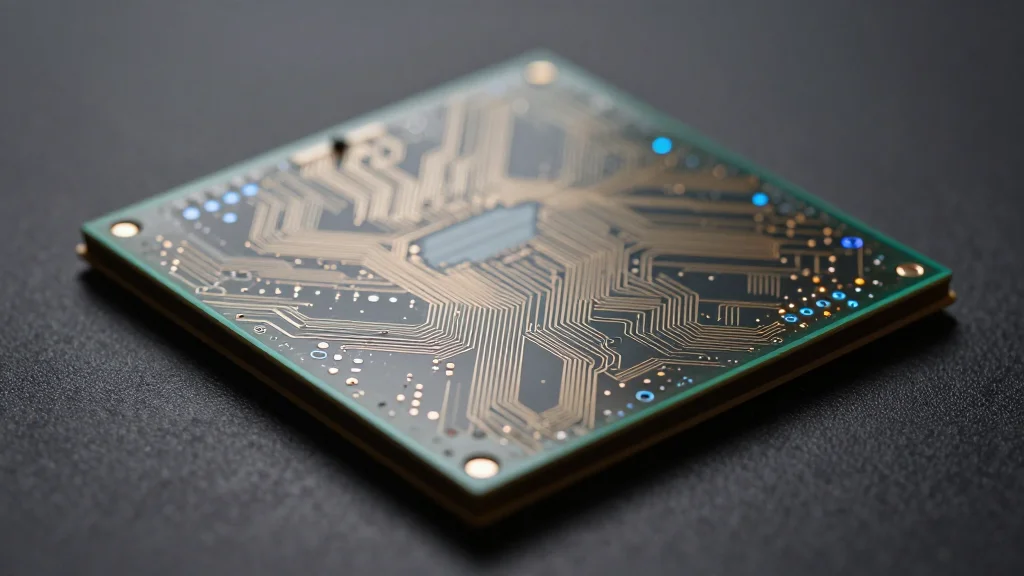
Diffuse electron projection lithography (DEPL) tackles that gap by replacing the traditional focused beam with a wide, diffuse electron stream that propagates in ambient air. The process employs a monolayer of gold nanoparticles as a contact mask, allowing the electron dose to be transferred directly onto the resist without intermediate optics. In laboratory trials, DEPL produced 4 nm line‑space patterns and processed 15 four‑inch wafers per hour; scaling calculations suggest a potential 532 twelve‑inch wafers per hour, rivaling current optical tools. The air‑based exposure eliminates costly ultra‑high‑vacuum chambers and simplifies equipment design, dramatically reducing capital outlay and operational overhead.
If DEPL matures to production readiness, it could reshape the cost structure of advanced node fabs. Chipmakers would gain a pathway to sub‑5 nm geometries without the massive EUV source investments, accelerating time‑to‑market for next‑generation processors and memory. Moreover, the decoupled resolution‑throughput relationship opens opportunities for rapid prototyping and low‑volume high‑performance devices, such as quantum‑computing chips or specialized AI accelerators. Industry analysts will watch the upcoming peer‑review validation and pilot line demonstrations closely, as DEPL’s promise of high‑resolution, high‑throughput, and low‑cost lithography could become a pivotal lever in the post‑EUV era.
High-Throughput Diffuse Electron Projection Lithography
Comments
Want to join the conversation?
Loading comments...