How Intel Foundry Packaging Technologies Redefine AI and HPC Scalability Limits
Companies Mentioned
Why It Matters
These innovations lower cost, power and risk while expanding the size and performance envelope of data‑center chips, accelerating the rollout of AI accelerators and exascale HPC platforms.
Key Takeaways
- •EMIB‑T scales packages to 120 mm × 120 mm, 9× reticles.
- •EMIB‑T achieves 12 Gb/s HBM4e and 64 Gb/s UCIe bandwidth.
- •Co‑packaged optics use glass couplers for low‑loss, detachable links.
- •Glass substrates with TGVs provide warpage‑free, high‑density interconnects.
- •Intel Foundry’s packaging cuts cost and power for AI/HPC.
Pulse Analysis
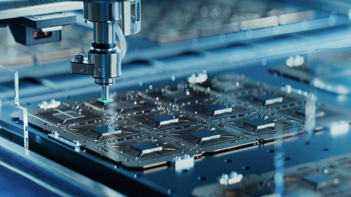
Intel’s EMIB‑T (Embedded Multi‑die Interconnect Bridge‑T) redefines chiplet integration by merging lateral 2.5D bridges with vertical TSV pathways. This hybrid approach lets designers stitch together multiple silicon reticles into a single, monolithic‑like package without the prohibitive cost of full‑die monolithics. The result is a 120 mm square form factor that can host more than nine compute or memory dies, delivering up to 64 Gb/s over the Universal Chiplet Interconnect Express (UCIe) and 12 Gb/s for HBM4e. For AI accelerators that demand massive bandwidth and low latency, EMIB‑T offers a scalable, cost‑effective bridge between performance and manufacturability.
Meanwhile, co‑packaged optics (CPO) tackles the bandwidth bottleneck that plagues traditional electrical interconnects in dense data‑center racks. By moving the optical‑to‑electrical conversion directly into the package and employing rigid glass fan‑out couplers with V‑groove edge coupling, Intel reduces insertion loss and simplifies assembly. The detachable edge connector design supports high‑volume production while maintaining the energy efficiency needed for AI‑scale networks. This optical integration not only trims power consumption but also opens a path to terabit‑per‑second fabric links without the thermal penalties of copper‑heavy designs.
Looking ahead, Intel’s shift to glass core substrates with through‑glass vias (TGVs) addresses the warpage and signal‑integrity challenges of organic laminates. Glass provides a flat, thermally stable platform that can host dense copper‑filled vias, enabling precise alignment for multi‑chiplet stacks and even optical routing on the same substrate. The durability of glass under aggressive thermal cycling ensures long‑term reliability for exascale HPC systems. Together, these packaging breakthroughs position Intel Foundry as a pivotal enabler for the next wave of AI and HPC hardware, where larger, faster, and more power‑efficient modules are essential for competitive advantage.
How Intel Foundry Packaging Technologies Redefine AI and HPC Scalability Limits
Comments
Want to join the conversation?
Loading comments...