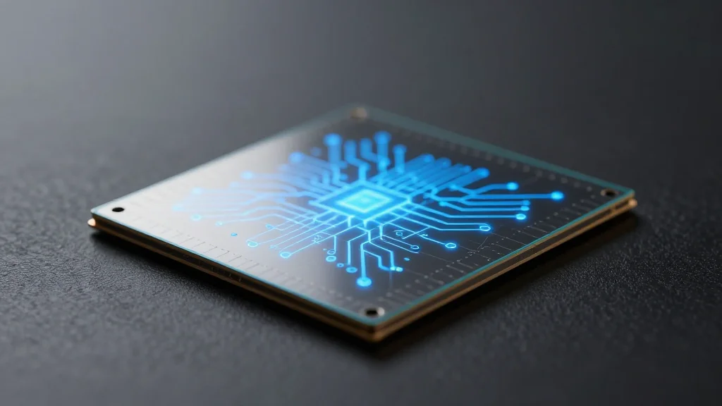
Imec Explores the Future of AI Hardware
Companies Mentioned
Why It Matters
The roadmap and foundry breakthroughs signal a new era of ultra‑dense, power‑efficient AI chips, essential for emerging workloads from edge HPC to autonomous vehicles. Accelerated AI‑driven design tools and higher‑NA lithography will help the industry meet the unprecedented demand that is pushing the market past the $1 trillion threshold.
Key Takeaways
- •imec roadmap targets A2 node with 0.75 NA EUV by 2041
- •Samsung HBM offers 2.8× power‑efficiency improvement
- •TSMC 2nm chips slated for 2026 smartphones
- •AI‑enhanced EDA tools add Z‑dimension for XTCO design
Pulse Analysis
The AI hardware landscape is entering a pivotal phase where power constraints and transistor density dictate the next wave of innovation. imec’s 15‑year CMOS roadmap, presented at ITF World, projects the adoption of hyper‑NA EUV lithography and sequential CFET devices by 2041, promising unprecedented scaling while keeping energy budgets in check. This forward‑looking vision underscores the need for cross‑technology co‑optimization (XTCO), linking advanced silicon, photonic interconnects, and system‑level design to unlock the performance required for future AI workloads.
Foundries are already moving to meet that vision. TSMC announced that its 2 nm process will power smartphones as early as 2026, and its CoWoS packaging will soon accommodate 50× more transistors per module. Samsung highlighted custom high‑bandwidth memory that delivers a 2.8‑fold boost in power efficiency, while Murata’s advanced module packaging is gaining traction in high‑performance computing. Meanwhile, ASML’s high‑NA EUV roadmap, featuring more powerful sources and modular tools, aims to alleviate the capacity bottleneck that could otherwise throttle AI‑driven demand, which industry analysts expect to push semiconductor revenues beyond $1 trillion by 2026.
Beyond silicon, AI is reshaping the design ecosystem itself. Cadence’s partnership with imec is delivering agentic EDA tools that incorporate a Z‑dimension, enabling designers to explore three‑dimensional placement and thermal optimization more effectively. AI‑accelerated material simulators are cutting discovery cycles from decades to days, opening pathways for novel substrates and superconducting circuits. Together, these advances are poised to support emerging physical‑AI applications—such as Rivian’s autonomous driving computers delivering 800 TOPS today and 1,600 TOPS tomorrow—by delivering deterministic, low‑latency hardware that moves intelligence from centralized clouds to the edge.
Imec Explores the Future of AI Hardware
Comments
Want to join the conversation?
Loading comments...