Imec Receives World’s Most Advanced High NA EUV System
Why It Matters
The system accelerates Europe’s push into next‑generation semiconductor nodes, giving AI and HPC developers a critical edge in performance and density. Early access also strengthens imec’s role as a collaborative R&D platform for global chip makers.
Key Takeaways
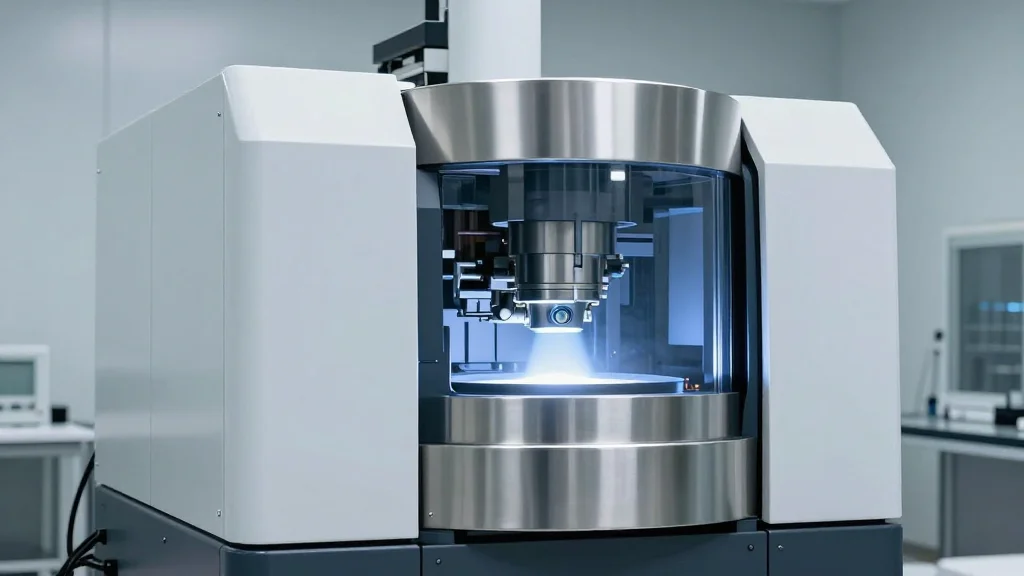
- •imec installs ASML EXE:5200, most advanced High NA EUV tool
- •Enables sub‑2 nm logic and high‑density memory research
- •Strengthens Europe’s semiconductor R&D leadership via EU funding
- •Provides partners early access to angstrom‑era lithography
- •Tool slated for full qualification by Q4 2026
Pulse Analysis
High Numerical Aperture (NA) Extreme Ultraviolet (EUV) lithography represents the latest leap in patterning technology, shrinking feature sizes beyond the capabilities of conventional EUV tools. ASML’s EXE:5200 pushes NA to 0.55, delivering finer resolution and higher throughput essential for sub‑2 nm nodes. By housing this system, imec not only gains a competitive research platform but also creates a testbed for new resists, mask designs, and metrology techniques that will define the next generation of logic and memory chips.
Europe’s semiconductor roadmap has long emphasized strategic autonomy, and the imec‑ASML collaboration is a cornerstone of that ambition. Funded by the EU’s Chips Joint Undertaking, the Flemish and Dutch governments, the project aligns with the NanoIC pilot line to cement the continent’s position in advanced R&D. imec’s extensive ecosystem—spanning chip manufacturers, equipment suppliers, and material innovators—facilitates rapid learning cycles, reducing time‑to‑market for breakthrough processes and counterbalancing the dominance of US and Asian fabs.
The practical impact of the EXE:5200 extends to high‑performance computing, artificial intelligence, and data‑center workloads that demand ever‑greater transistor density and energy efficiency. As imec targets full qualification by the fourth quarter of 2026, partners will begin to prototype designs that exploit the angstrom‑scale precision, potentially unlocking new architectures for AI accelerators and high‑bandwidth memory. This early access not only accelerates product development but also cultivates a talent pipeline versed in cutting‑edge lithography, reinforcing Europe’s long‑term competitiveness in the global semiconductor arena.
imec Receives World’s Most Advanced High NA EUV System
Comments
Want to join the conversation?
Loading comments...