Imec Unveils Quantum Dot Qubit Device Using High NA EUV Lithography
Why It Matters
By marrying quantum dot qubits with advanced EUV patterning, imec creates a manufacturable path to the massive qubit counts required for practical quantum computers, accelerating the race for quantum advantage.
Key Takeaways
- •First integrated quantum device made with High NA EUV lithography
- •6‑nm gate gaps enable dense, low‑noise silicon spin qubits
- •Process aligns with 300 mm CMOS fab standards for scalability
- •Silicon qubits leverage existing semiconductor ecosystem, reducing development cost
- •Millions of qubits could fit on a single chip theoretically
Pulse Analysis
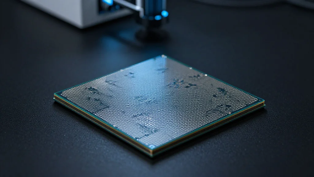
High Numerical Aperture (NA) extreme ultraviolet (EUV) lithography has been the engine behind the latest generation of sub‑2 nm logic chips, but imec’s recent demonstration shows its relevance beyond classical computing. By using ASML’s High NA EUV tools, imec patterned silicon quantum‑dot structures with 6 nm gaps, a precision level previously unattainable for quantum hardware. This breakthrough proves that the same photolithography infrastructure that fuels AI accelerators can also produce the ultra‑fine features needed to control electron spin states, bridging two historically separate technology roadmaps.
Silicon quantum‑dot spin qubits are prized for their compatibility with existing CMOS processes, allowing the semiconductor industry’s massive design‑for‑manufacturing ecosystem to be repurposed for quantum applications. The imec device demonstrates low charge noise and stable operation, key metrics for qubit fidelity, while maintaining a fab‑compatible 300 mm wafer format. Such alignment reduces the need for bespoke, low‑volume quantum fabs and opens the door to leveraging mature supply chains, automated testing, and volume‑based cost reductions that have driven Moore’s Law for decades.
The strategic impact of this development is profound. Scaling quantum computers to the millions of qubits required for fault‑tolerant operation has been a major bottleneck; imec’s High NA EUV approach directly addresses the lithographic limitation, enabling dense qubit packing without sacrificing coherence. As major chipmakers and cloud providers race to offer quantum services, a manufacturable silicon‑based platform could become the industry standard, accelerating commercialization and widening the ecosystem of quantum software and hardware partners. The convergence of advanced lithography and quantum engineering signals a pivotal shift toward practical, large‑scale quantum computing.
imec Unveils Quantum Dot Qubit Device Using High NA EUV Lithography
Comments
Want to join the conversation?
Loading comments...