Intel Charges Ahead With New Process Nodes
Companies Mentioned
Why It Matters
Intel’s accelerated node roadmap repositions it against TSMC and Samsung, promising new design opportunities and reinforcing its fab‑as‑a‑service ambitions. Early PDK access helps customers validate yields, accelerating time‑to‑market for advanced chips.
Key Takeaways
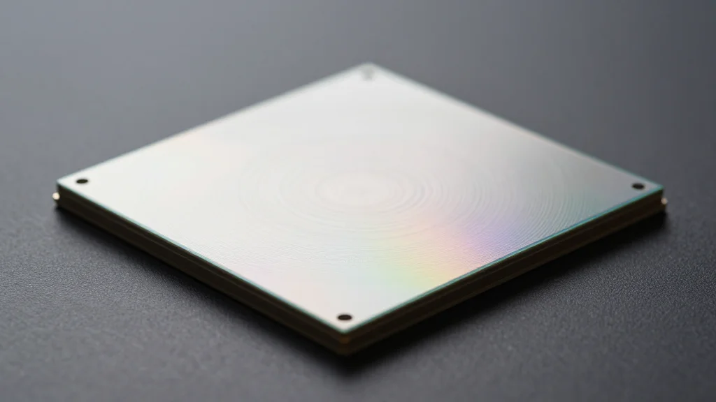
- •Intel's 18A node entered full‑volume production in 2024
- •14A PDK version 0.5 released; version 0.9 due October
- •14A volume production targeted for 2028
- •Roadmap adds 10A and 7A nodes within next decade
- •Early PDK access lets customers test yield and designs
Pulse Analysis
Intel’s latest milestone—full‑scale production of its 18A (1.8 nm) process—marks a turning point after years of lagging behind industry leaders. The 18A node delivers higher transistor density and lower power consumption, key metrics for data‑center and AI workloads. By delivering a functional PDK at version 0.5, Intel signals that its manufacturing stack is mature enough for customers to begin design validation, a crucial step toward securing early silicon orders.
The company’s roadmap now publicly includes 14A, 10A and 7A nodes, with the 14A PDK version 0.9 slated for an October release and volume production not expected before 2028. This timeline puts Intel in direct competition with TSMC’s N3 and N2 processes and Samsung’s 3 nm offerings. While Intel’s node naming differs, the underlying goal is comparable: shrink transistor gate lengths to improve performance per watt. The early PDK rollout gives design houses a chance to benchmark Intel’s yield characteristics against rivals, potentially shifting some fab‑as‑a‑service business toward Intel’s IDM 2.0 model.
For customers, the significance lies in the ability to plan multi‑year product cycles around a predictable technology roadmap. Access to the 0.9 PDK before silicon fab ramp‑up enables early architectural exploration, reducing risk and shortening time‑to‑market for next‑generation AI accelerators and high‑performance compute chips. Moreover, Intel’s commitment to a decade‑long node progression suggests sustained capital investment in its U.S. and European fabs, which could reshape supply‑chain dynamics and offer a domestic alternative to Asian foundries. As the semiconductor industry grapples with capacity constraints, Intel’s aggressive node strategy may become a catalyst for broader ecosystem growth.
Intel Charges Ahead With New Process Nodes
Comments
Want to join the conversation?
Loading comments...