JEDEC Releases New Memory Interface Logic and Expanded MRDIMM Roadmap
Why It Matters
The new standards tighten signal integrity and boost data rates, enabling servers and AI accelerators to meet exploding memory bandwidth demands. Early adoption will give OEMs a competitive edge in data‑intensive markets.
Key Takeaways
- •JEDEC published DDR5MDB02 standard for multiplexed rank data buffers.
- •Upcoming DDR5MRCD02 will improve clock driver signal integrity.
- •MRDIMM Gen2 roadmap targets 12,800 MT/s raw card speeds.
- •Gen3 MRDIMM development aims for future high‑bandwidth servers.
- •New standards enable scalable DDR5 memory for data‑intensive workloads.
Pulse Analysis
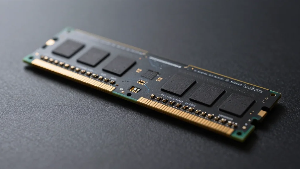
JEDEC’s latest releases mark a pivotal step in the evolution of DDR5 memory, a technology that underpins everything from cloud data centers to high‑performance computing clusters. By formalizing the DDR5MDB02 multiplexed rank data buffer, the industry gains a common framework for handling the increased parallelism of modern DIMM architectures. This standard not only clarifies electrical specifications but also paves the way for more reliable scaling as memory bandwidth pushes beyond current limits.
The forthcoming DDR5MRCD02 clock‑driver specification complements the data‑buffer standard by tightening timing margins and enhancing signal integrity across densely packed memory channels. Coupled with the near‑final MRDIMM Gen2 module definition, designers can now target raw‑card speeds of 12,800 MT/s—a rate that translates to roughly 102 GB/s per channel in a dual‑rank configuration. Such performance is critical for AI training workloads, real‑time analytics, and next‑generation enterprise servers that demand low latency and high throughput. Early silicon prototypes already demonstrate the feasibility of these speeds, suggesting a rapid path from specification to product.
Looking ahead, JEDEC’s Gen3 MRDIMM roadmap signals an ambition to sustain the momentum of DDR5 scaling well into the next decade. As data‑centric applications continue to grow, memory manufacturers will need to adopt these standards to stay competitive. The industry timeline points to initial Gen2 adoption in 2025, with Gen3 designs expected by 2027, aligning with the rollout of new processor generations that can fully exploit the expanded bandwidth. Stakeholders—from silicon vendors to system integrators—should monitor JEDEC’s publications closely to align product roadmaps and capitalize on the performance gains these standards promise.
JEDEC Releases New Memory Interface Logic and Expanded MRDIMM Roadmap
Comments
Want to join the conversation?
Loading comments...