Companies Mentioned
Why It Matters
A coordinated SIG accelerates MRAM’s move from niche to mainstream, reducing technical risk and fostering standards that unlock new high‑performance, non‑volatile memory applications.
Key Takeaways
- •MRAM Alliance SIG launched under SNIA to unify ecosystem
- •STT‑MRAM now in major foundries like TSMC and Samsung
- •Embedded MRAM adopted for automotive MCUs, offering radiation tolerance
- •Magnetic immunity concerns addressed via testing standards and shielding
- •Goal: drive standards and adoption across data center, AI, edge
Pulse Analysis
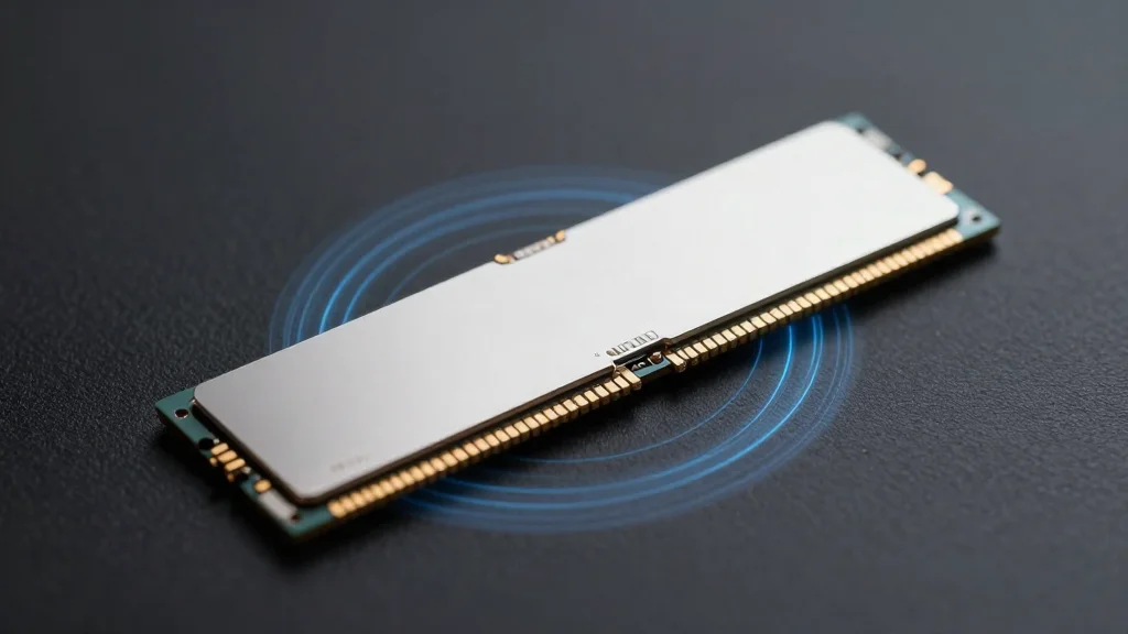
The formation of the MRAM Alliance Special Interest Group marks a watershed moment for magnetoresistive memory. After years of research, spin‑transfer torque (STT) MRAM has achieved production‑grade yields at leading fabs such as TSMC, Samsung, UMC and GlobalFoundries. By nesting the SIG within SNIA, the initiative taps a broad base of end‑users and semiconductor partners, creating a single forum to share roadmaps, address supply‑chain gaps, and promote the technology’s unique blend of speed, endurance and non‑volatility. This collaborative structure is designed to fast‑track MRAM’s transition from specialty niches to broader commercial adoption.
Technical skepticism, especially around magnetic immunity, has slowed market confidence. The SIG is tackling these concerns head‑on by endorsing IEEE‑defined magnetic‑field testing, encouraging package‑level shielding, and advocating for a JEDEC‑style interface standard that would simplify system‑level integration. By codifying performance thresholds and providing clear qualification pathways, the group reduces design risk for OEMs and helps differentiate MRAM from competing non‑volatile memories like flash and ReRAM, which lack the same combination of fast read/write latency and infinite endurance.
From a business perspective, MRAM’s attributes open new opportunities across high‑growth segments. Automotive microcontrollers are already replacing NOR flash with embedded MRAM to gain radiation tolerance and instant‑on capability, while space‑qualified devices benefit from its resilience to harsh environments. In data‑center and edge AI workloads, MRAM can alleviate memory bottlenecks by enabling on‑chip inference with non‑volatile, low‑latency storage, potentially lowering power consumption and improving system uptime. As the SIG matures standards and educates the market, MRAM is poised to become a cornerstone of next‑generation computing architectures.
MRAM Gets Its Own SIG
Comments
Want to join the conversation?
Loading comments...