Near-Zero-CTE Dielectric Targets 224 Gb/S AI Links
Why It Matters
These dielectrics address thermomechanical mismatch in large AI accelerators, enabling higher data rates and longer product lifespans, which is critical as AI hardware scales in size and speed.
Key Takeaways
- •HM50 CTE –8 ppm/°C offsets copper expansion in AI PCBs
- •Board warpage drops 64% on large AI accelerator platforms
- •Package bow reduced 81%, extending overall system reliability
- •Solder‑fatigue life improves over 100× versus standard PCB
- •HM001 offers Dk 2.90, Df 0.001 for ultra‑low loss
Pulse Analysis
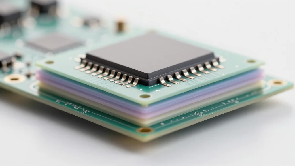
The rapid expansion of AI workloads has pushed board‑level designs into regimes where traditional dielectric materials struggle to keep pace. As data rates climb toward 224 Gb/s, even modest thermal expansion mismatches between copper traces and substrate can cause warpage, signal distortion, and premature solder fatigue. Engineers therefore seek materials with coefficients of thermal expansion (CTE) that not only match but actively counteract copper’s expansion, preserving dimensional stability across the wide temperature swings typical in data‑center environments.
Celeritas HM50 and HM001 answer that need with engineered CTEs of –8 ppm/°C and near‑zero, respectively. HM50’s negative CTE actively offsets copper’s positive expansion, delivering a 64% reduction in board warpage and an 81% drop in package bow on large‑format AI accelerator platforms. The resulting mechanical stability translates into more than a 100‑fold increase in solder‑fatigue life, a metric that directly impacts maintenance cycles and total cost of ownership. Meanwhile, HM001’s ultra‑low dielectric loss (Df ≈ 0.001) and moderate permittivity (Dk ≈ 2.90) make it ideal for high‑frequency signal layers where loss directly erodes link budget.
The introduction of these materials signals a broader shift toward thermomechanically aware design in the AI hardware ecosystem. As AI chips grow larger and operate at higher speeds, manufacturers will increasingly prioritize substrates that can mitigate thermal stress while preserving signal integrity. Competitors are likely to accelerate R&D into similar low‑CTE, low‑loss dielectrics, potentially spurring a new standards race for AI‑grade PCBs. Early adopters of HM50 and HM001 could gain a competitive edge by delivering more reliable, higher‑performance systems, reinforcing the strategic importance of material innovation in the next generation of AI infrastructure.
Near-zero-CTE dielectric targets 224 Gb/s AI links
Comments
Want to join the conversation?
Loading comments...